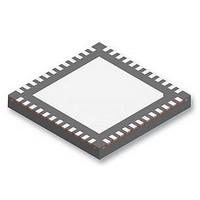
DS92LV2421SQE/NOPB National Semiconductor, DS92LV2421SQE/NOPB Datasheet - Page 6

DS92LV2421SQE/NOPB
Manufacturer Part Number
DS92LV2421SQE/NOPB
Description
IC SER/DESER 10-75MHZ 24B 48LLP
Manufacturer
National Semiconductor
Datasheet
1.DS92LV2421SQENOPB.pdf
(40 pages)
Specifications of DS92LV2421SQE/NOPB
Serdes Function
Serialiser
Ic Input Type
LVCMOS
Ic Output Type
CML
No. Of Inputs
1
No. Of Outputs
1
Supply Voltage Range
1.71V To 1.89V
Driver Case Style
LLP
No. Of Pins
48
Svhc
No SVHC
Rohs Compliant
Yes
Lead Free Status / RoHS Status
Lead free / RoHS Compliant
Other names
DS92LV2421SQE/NOPBTR
Available stocks
Company
Part Number
Manufacturer
Quantity
Price
Company:
Part Number:
DS92LV2421SQE/NOPB
Manufacturer:
NSC
Quantity:
1 250
Part Number:
DS92LV2421SQE/NOPB
Manufacturer:
TI/德州仪器
Quantity:
20 000
www.national.com
Pin Name
CO1
CO2
CO3
CLKOUT
LOCK
PASS
Control and Configuration — STRAP PINS
For a High State, use a 10 kΩ pull up to V
power-up and set device configuration. Pin Number listed along with shared data output name in square brackets.
CONFIG[1:0]
LF_MODE
OS_CLKOUT
10 [DO22],
12 [DO20]
11 [DO21]
9 [DO23]
Pin #
32
42
6
8
7
5
O, LVCMOS Control Signal Output
O, LVCMOS Control Signal Output
O, LVCMOS Control Signal Output
O, LVCMOS Pixel Clock Output
O, LVCMOS LOCK Status Output
O, LVCMOS PASS Output (BIST Mode)
w/ pull-down
w/ pull-down
w/ pull-down
I, LVCMOS
I, LVCMOS
I, LVCMOS
I/O, Type
STRAP
STRAP
STRAP
DDIO
Description
For Display/Video Application:
CO1 = Data Enable Output
Control signal pulse width must be 3 clocks or longer to be transmitted when the Control
Signal Filter is enabled (CONFIG[1:0] = 01). There is no restriction on the minimum transition
pulse when the Control Signal Filter is disabled (CONFIG[1:0] = 00).
The signal is limited to 2 transitions per 130 clocks regardless of the Control Signal Filter
setting.
In power-down (PDB = 0), output is controlled by the OSS_SEL pin (See
For Display/Video Application:
CO2 = Horizontal Sync Output
Control signal pulse width must be 3 clocks or longer to be transmitted when the Control
Signal Filter is enabled (CONFIG[1:0] = 01). There is no restriction on the minimum transition
pulse when the Control Signal Filter is disabled (CONFIG[1:0] = 00).
The signal is limited to 2 transitions per 130 clocks regardless of the Control Signal Filter
setting.
In power-down (PDB = 0), output is controlled by the OSS_SEL pin (See
For Display/Video Application:
CO3 = Vertical Sync Output
CO3 is different than CO1 and CO2 because it is limited to 1 transition per 130 clock cycles.
Thus, the minimum pulse width allowed is 130 clock cycle wide.
The CONFIG[1:0] pins have no affect on CO3 signal
In power-down (PDB = 0), output is controlled by the OSS_SEL pin (See
In power-down (PDB = 0), output is controlled by the OSS_SEL pin (See
strobe edge set by RFB.
LOCK = 1, PLL is Locked, outputs are active LOCK = 0, PLL is unlocked, DO[23:0], CO1,
CO2, CO3 and CLKOUT output states are controlled by OSS_SEL (See
used as Link Status or to flag when Video Data is active (ON/OFF).
PASS = 1, error free transmission
PASS = 0, one or more errors were detected in the received payload
Route to test point for monitoring, or leave open if unused.
00: Control Signal Filter DISABLED
01: Control Signal Filter ENABLED
10: Reverse compatibility mode to interface with the DS90UR241 or DS99R241
11: Reverse compatibility mode to interface with the DS90C241
SSCG Low Frequency Mode
Only required when SSCG is enabled, otherwise LF_MODE condition is a DON’T CARE
(X).
LF_MODE = 1, SSCG in low frequency mode (CLK = 10-20 MHz)
LF_MODE = 0, SSCG in high frequency mode (CLK = 20-65 MHz)
This can also be controlled by I2C register access.
Output CLKOUT Slew Select
OS_CLKOUT = 1, Increased CLKOUT slew rate
OS_CLKOUT = 0, Normal CLKOUT slew rate (default)
This can also be controlled by I2C register access.
; for a Low State, the IO includes an internal pull down. The STRAP pins are read upon
6
Table
Table
Table
Table
Table
8). May be
8).
8).
8).
8). Data


