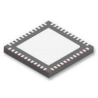
DS92LV2421SQE/NOPB National Semiconductor, DS92LV2421SQE/NOPB Datasheet - Page 4

DS92LV2421SQE/NOPB
Manufacturer Part Number
DS92LV2421SQE/NOPB
Description
IC SER/DESER 10-75MHZ 24B 48LLP
Manufacturer
National Semiconductor
Datasheet
1.DS92LV2421SQENOPB.pdf
(40 pages)
Specifications of DS92LV2421SQE/NOPB
Serdes Function
Serialiser
Ic Input Type
LVCMOS
Ic Output Type
CML
No. Of Inputs
1
No. Of Outputs
1
Supply Voltage Range
1.71V To 1.89V
Driver Case Style
LLP
No. Of Pins
48
Svhc
No SVHC
Rohs Compliant
Yes
Lead Free Status / RoHS Status
Lead free / RoHS Compliant
Other names
DS92LV2421SQE/NOPBTR
Available stocks
Company
Part Number
Manufacturer
Quantity
Price
Company:
Part Number:
DS92LV2421SQE/NOPB
Manufacturer:
NSC
Quantity:
1 250
Part Number:
DS92LV2421SQE/NOPB
Manufacturer:
TI/德州仪器
Quantity:
20 000
www.national.com
Pin Name
CLKIN
Control and Configuration
PDB
VODSEL
De-Emph
RFB
CONFIG
[1:0]
ID[x]
SCL
SDA
BISTEN
RES[2:0]
Channel-Link II — CML Serial Interface
DOUT+
DOUT-
Power and Ground (see NOTE below)
VDDL
VDDP
VDDHS
VDDTX
VDDIO
GND
NOTE: 1= HIGH, 0 L= LOW
The VDD (V
on the PDB pin is needed to ensure PDB arrives after all the VDD have settled to the recommended operating voltage.
DDn
18, 16, 15
13, 12
Pin #
DAP
and V
10
21
24
23
11
31
20
19
14
17
22
30
6
8
9
7
DDIO
) supply ramp should be faster than 1.5 ms with a monotonic rise. If slower then 1.5 ms then a capacitor
I/O, LVCMOS
w/ pull-down
w/ pull-down
w/ pull-down
w/ pull-down
w/ pull-down
w/ pull-down
w/ pull-down
I, LVCMOS
I, LVCMOS
I, LVCMOS
I, LVCMOS
I, LVCMOS
I, LVCMOS
Open Drain
I, LVCMOS
I, LVCMOS
I/O, Type
w/ pull-up
I, Analog
I, Analog
O, CML
O, CML
Ground
Power
Power
Power
Power
Power
Description
Clock Input
Latch/data strobe edge set by RFB pin.
Power-down Mode Input
PDB = 1, Ser is enabled (normal operation).
Refer to ”Power Up Requirements and PDB Pin” in the Applications Information Section.
PDB = 0, Ser is powered down. When the Ser is in the power-down state, the driver outputs
(DOUT+/-) are both logic high, the PLL is shutdown, IDD is minimized. Control Registers
are RESET.
Differential Driver Output Voltage Select (This is can also be control by I2C register.)
VODSEL = 1, LVDS VOD is ±420 mV, 840 mVp-p (typ) — long cable / De-Emph apps
VODSEL = 0, LVDS VOD is ±280 mV, 560 mVp-p (typ) — short cable (no De-emph), low
power mode.
De-Emphasis Control (This can also be controlled by I2C register access.)
De-Emph = open (float) - disabled
To enable De-emphasis, tie a resistor from this pin to GND or control via register.
See
Clock Input Latch/Data Strobe Edge Select (This can also be controlled by I2C register
access.)
RFB = 1, parallel interface data and control signals are latched on the rising clock edge.
RFB = 0, parallel interface data and control signals are latched on the falling clock edge.
00: Control Signal Filter DISABLED
01: Control Signal Filter ENABLED
10: Reverse compatibility mode to interface with the DS90UR124 or DS99R124Q
11: Reverse compatibility mode to interface with the DS90C124
I2C Serial Control Bus Device ID Address Select — Optional
Resistor to Ground and 10 kΩ pull-up to 1.8V rail. See
I2C Serial Control Bus Clock Input - Optional
SCL requires an external pull-up resistor to V
I2C Serial Control Bus Data Input / Output - Optional
SDA requires an external pull-up resistor V
BIST Mode — Optional
BISTEN = 0, BIST is disabled (normal operation)
BISTEN = 1, BIST is enabled
Reserved - tie LOW
Non–Inverting Output.
The output must be AC Coupled with a 0.1 µF capacitor.
Inverting Output.
The output must be AC Coupled with a 0.1 µF capacitor.
Logic Power, 1.8 V ±5%
PLL Power, 1.8 V ±5%
TX High Speed Logic Power, 1.8 V ±5%
Output Driver Power, 1.8 V ±5%
LVCMOS I/O Power, 1.8 V ±5% OR 3.3 V ±10%
DAP is the large metal contact at the bottom side, located at the center of the LLP
package. Connect to the ground plane (GND) with at least 9 vias.
Table
4.
4
DDIO
DDIO
.
.
Table
11.


