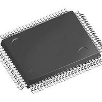
LFXP3C-3QN208C Lattice, LFXP3C-3QN208C Datasheet - Page 10

LFXP3C-3QN208C
Manufacturer Part Number
LFXP3C-3QN208C
Description
FPGA - Field Programmable Gate Array 3.1K LUTS 136 I/O
Manufacturer
Lattice
Datasheet
1.LFXP3C-3QN208C.pdf
(130 pages)
Specifications of LFXP3C-3QN208C
Number Of Macrocells
3000
Maximum Operating Frequency
320 MHz
Number Of Programmable I/os
136
Data Ram Size
55296
Supply Voltage (max)
3.465 V
Maximum Operating Temperature
+ 90 C
Minimum Operating Temperature
0 C
Mounting Style
SMD/SMT
Supply Voltage (min)
1.71 V
Package / Case
PQFP-208
Lead Free Status / RoHS Status
Lead free / RoHS Compliant
Available stocks
Company
Part Number
Manufacturer
Quantity
Price
Company:
Part Number:
LFXP3C-3QN208C
Manufacturer:
Lattice
Quantity:
135
Company:
Part Number:
LFXP3C-3QN208C
Manufacturer:
LOGIC
Quantity:
4
Company:
Part Number:
LFXP3C-3QN208C
Manufacturer:
LATTICE
Quantity:
1 360
Company:
Part Number:
LFXP3C-3QN208C
Manufacturer:
Lattice Semiconductor Corporation
Quantity:
10 000
Part Number:
LFXP3C-3QN208C
Manufacturer:
LATTICE
Quantity:
20 000
Lattice Semiconductor
Figure 2-5. Primary Clock Sources
Secondary Clock Sources
LatticeXP devices have four secondary clock resources per quadrant. The secondary clock branches are tapped at
every PFU. These secondary clock networks can also be used for controls and high fanout data. These secondary
clocks are derived from four clock input pads and 16 routing signals as shown in Figure 2-6.
Clock Input
PLL Input
PLL Input
Note: Smaller devices have two PLLs.
PLL
PLL
From Routing
From Routing
To Quadrant Clock Selection
20 Primary Clock Sources
Clock Input
Clock Input
2-7
From Routing
From Routing
LatticeXP Family Data Sheet
PLL
PLL
PLL Input
Clock Input
PLL Input
Architecture


