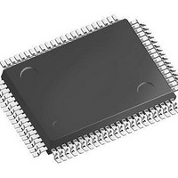
LFXP3C-3QN208C Lattice, LFXP3C-3QN208C Datasheet - Page 62

LFXP3C-3QN208C
Manufacturer Part Number
LFXP3C-3QN208C
Description
FPGA - Field Programmable Gate Array 3.1K LUTS 136 I/O
Manufacturer
Lattice
Datasheet
1.LFXP3C-3QN208C.pdf
(130 pages)
Specifications of LFXP3C-3QN208C
Number Of Macrocells
3000
Maximum Operating Frequency
320 MHz
Number Of Programmable I/os
136
Data Ram Size
55296
Supply Voltage (max)
3.465 V
Maximum Operating Temperature
+ 90 C
Minimum Operating Temperature
0 C
Mounting Style
SMD/SMT
Supply Voltage (min)
1.71 V
Package / Case
PQFP-208
Lead Free Status / RoHS Status
Lead free / RoHS Compliant
Available stocks
Company
Part Number
Manufacturer
Quantity
Price
Company:
Part Number:
LFXP3C-3QN208C
Manufacturer:
Lattice
Quantity:
135
Company:
Part Number:
LFXP3C-3QN208C
Manufacturer:
LOGIC
Quantity:
4
Company:
Part Number:
LFXP3C-3QN208C
Manufacturer:
LATTICE
Quantity:
1 360
Company:
Part Number:
LFXP3C-3QN208C
Manufacturer:
Lattice Semiconductor Corporation
Quantity:
10 000
Part Number:
LFXP3C-3QN208C
Manufacturer:
LATTICE
Quantity:
20 000
Lattice Semiconductor
PICs and DDR Data (DQ) Pins Associated with the DDR Strobe (DQS) Pin
P[Edge] [n-4]
P[Edge] [n-3]
P[Edge] [n-2]
P[Edge] [n-1]
P[Edge] [n]
P[Edge] [n+1]
P[Edge] [n+2]
P[Edge] [n+3]
Notes:
1. “n” is a row/column PIC number.
2. The DDR interface is designed for memories that support one DQS strobe per eight bits of data. In some packages, all the potential DDR
3. The definition of the PIC numbering is provided in the Signal Names column of the Signal Descriptions table in this data sheet.
data (DQ) pins may not be available.
with DQS Strobe
PICs Associated
PIO within PIC
A
B
A
B
A
B
A
B
A
B
A
B
A
B
4-3
Complement
Complement
Complement
Complement
Complement
Complement
Complement
Polarity
True
True
True
True
True
True
True
LatticeXP Family Data Sheet
Pinout Information
and Data (DQ) Pins
DDR Strobe (DQS)
[Edge]DQSn
DQ
DQ
DQ
DQ
DQ
DQ
DQ
DQ
DQ
DQ
DQ
DQ
DQ


