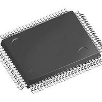
LFXP3C-3QN208C Lattice, LFXP3C-3QN208C Datasheet - Page 25

LFXP3C-3QN208C
Manufacturer Part Number
LFXP3C-3QN208C
Description
FPGA - Field Programmable Gate Array 3.1K LUTS 136 I/O
Manufacturer
Lattice
Datasheet
1.LFXP3C-3QN208C.pdf
(130 pages)
Specifications of LFXP3C-3QN208C
Number Of Macrocells
3000
Maximum Operating Frequency
320 MHz
Number Of Programmable I/os
136
Data Ram Size
55296
Supply Voltage (max)
3.465 V
Maximum Operating Temperature
+ 90 C
Minimum Operating Temperature
0 C
Mounting Style
SMD/SMT
Supply Voltage (min)
1.71 V
Package / Case
PQFP-208
Lead Free Status / RoHS Status
Lead free / RoHS Compliant
Available stocks
Company
Part Number
Manufacturer
Quantity
Price
Company:
Part Number:
LFXP3C-3QN208C
Manufacturer:
Lattice
Quantity:
135
Company:
Part Number:
LFXP3C-3QN208C
Manufacturer:
LOGIC
Quantity:
4
Company:
Part Number:
LFXP3C-3QN208C
Manufacturer:
LATTICE
Quantity:
1 360
Company:
Part Number:
LFXP3C-3QN208C
Manufacturer:
Lattice Semiconductor Corporation
Quantity:
10 000
Part Number:
LFXP3C-3QN208C
Manufacturer:
LATTICE
Quantity:
20 000
Architecture
Lattice Semiconductor
LatticeXP Family Data Sheet
Polarity Control Logic
In a typical DDR Memory interface design, the phase relation between the incoming delayed DQS strobe and the
internal system Clock (during the READ cycle) is unknown.
The LatticeXP family contains dedicated circuits to transfer data between these domains. To prevent setup and
hold violations at the domain transfer between DQS (delayed) and the system Clock a clock polarity selector is
used. This changes the edge on which the data is registered in the synchronizing registers in the input register
block. This requires evaluation at the start of the each READ cycle for the correct clock polarity.
Prior to the READ operation in DDR memories DQS is in tristate (pulled by termination). The DDR memory device
drives DQS low at the start of the preamble state. A dedicated circuit detects this transition. This signal is used to
control the polarity of the clock to the synchronizing registers.
sysIO Buffer
Each I/O is associated with a flexible buffer referred to as a sysIO buffer. These buffers are arranged around the
periphery of the device in eight groups referred to as Banks. The sysIO buffers allow users to implement the wide
variety of standards that are found in today’s systems including LVCMOS, SSTL, HSTL, LVDS and LVPECL.
sysIO Buffer Banks
LatticeXP devices have eight sysIO buffer banks; each is capable of supporting multiple I/O standards. Each sysIO
bank has its own I/O supply voltage (V
), and two voltage references V
and V
resources allowing each
CCIO
REF1
REF2
bank to be completely independent from each other. Figure 2-28 shows the eight banks and their associated sup-
plies.
In the LatticeXP devices, single-ended output buffers and ratioed input buffers (LVTTL, LVCMOS, PCI and PCI-X) are
powered using V
. LVTTL, LVCMOS33, LVCMOS25 and LVCMOS12 can also be set as a fixed threshold input
CCIO
independent of V
In addition to the bank V
supplies, the LatticeXP devices have a V
core logic power sup-
CCIO.
CCIO
CC
ply, and a V
supply that power all differential and referenced buffers.
CCAUX
Each bank can support up to two separate VREF voltages, VREF1 and VREF2 that set the threshold for the refer-
enced input buffers. In the LatticeXP devices, a dedicated pin in a bank can be configured to be a reference voltage
supply pin. Each I/O is individually configurable based on the bank’s supply and reference voltages.
2-22


