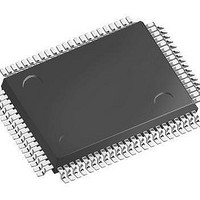
LFXP3C-3QN208C Lattice, LFXP3C-3QN208C Datasheet - Page 7

LFXP3C-3QN208C
Manufacturer Part Number
LFXP3C-3QN208C
Description
FPGA - Field Programmable Gate Array 3.1K LUTS 136 I/O
Manufacturer
Lattice
Datasheet
1.LFXP3C-3QN208C.pdf
(130 pages)
Specifications of LFXP3C-3QN208C
Number Of Macrocells
3000
Maximum Operating Frequency
320 MHz
Number Of Programmable I/os
136
Data Ram Size
55296
Supply Voltage (max)
3.465 V
Maximum Operating Temperature
+ 90 C
Minimum Operating Temperature
0 C
Mounting Style
SMD/SMT
Supply Voltage (min)
1.71 V
Package / Case
PQFP-208
Lead Free Status / RoHS Status
Lead free / RoHS Compliant
Available stocks
Company
Part Number
Manufacturer
Quantity
Price
Company:
Part Number:
LFXP3C-3QN208C
Manufacturer:
Lattice
Quantity:
135
Company:
Part Number:
LFXP3C-3QN208C
Manufacturer:
LOGIC
Quantity:
4
Company:
Part Number:
LFXP3C-3QN208C
Manufacturer:
LATTICE
Quantity:
1 360
Company:
Part Number:
LFXP3C-3QN208C
Manufacturer:
Lattice Semiconductor Corporation
Quantity:
10 000
Part Number:
LFXP3C-3QN208C
Manufacturer:
LATTICE
Quantity:
20 000
Lattice Semiconductor
Table 2-1. Slice Signal Descriptions
Modes of Operation
Each Slice is capable of four modes of operation: Logic, Ripple, RAM and ROM. The Slice in the PFF is capable of
all modes except RAM. Table 2-2 lists the modes and the capability of the Slice blocks.
Table 2-2. Slice Modes
Logic Mode: In this mode, the LUTs in each Slice are configured as 4-input combinatorial lookup tables. A LUT4
can have 16 possible input combinations. Any logic function with four inputs can be generated by programming this
lookup table. Since there are two LUT4s per Slice, a LUT5 can be constructed within one Slice. Larger lookup
tables such as LUT6, LUT7 and LUT8 can be constructed by concatenating other Slices.
Ripple Mode: Ripple mode allows the efficient implementation of small arithmetic functions. In ripple mode, the fol-
lowing functions can be implemented by each Slice:
Two additional signals: Carry Generate and Carry Propagate are generated per Slice in this mode, allowing fast
arithmetic functions to be constructed by concatenating Slices.
RAM Mode: In this mode, distributed RAM can be constructed using each LUT block as a 16x1-bit memory.
Through the combination of LUTs and Slices, a variety of different memories can be constructed.
• Addition 2-bit
• Subtraction 2-bit
• Add/Subtract 2-bit using dynamic control
• Up counter 2-bit
• Down counter 2-bit
• Ripple mode multiplier building block
• Comparator functions of A and B inputs
1. See Figure 2-2 for connection details.
2. Requires two PFUs.
Function
- A greater-than-or-equal-to B
- A not-equal-to B
- A less-than-or-equal-to B
Output
Output
Output
Output
Output
Input
Input
Input
Input
Input
Input
Input
Input
PFU Slice
PFF Slice
Inter-PFU signal
Inter-PFU signal
Multi-purpose
Multi-purpose
Control signal
Control signal
Control signal
Data signals
Data signals
Data signals
Data signals
Data signal
Data signal
Type
LUT 4x2 or LUT 5x1
LUT 4x2 or LUT 5x1
Logic
A0, B0, C0, D0 Inputs to LUT4
A1, B1, C1, D1 Inputs to LUT4
Signal Names
Q0, Q1
F0, F1
OFX0
OFX1
FCIN
FCO
LSR
CLK
M0
M1
CE
2-bit Arithmetic Unit
2-bit Arithmetic Unit
Multipurpose Input
Multipurpose Input
Clock Enable
Local Set/Reset
System Clock
Fast Carry In
LUT4 output register bypass signals
Register Outputs
Output of a LUT5 MUX
Output of a LUT6, LUT7, LUT8
For the right most PFU the fast carry chain output
2-4
Ripple
1
Description
SP 16x2
RAM
LatticeXP Family Data Sheet
N/A
2
MUX depending on the slice
ROM 16x1 x 2
ROM 16x1 x 2
ROM
1
Architecture


