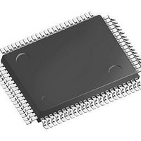
LFXP3C-3QN208C Lattice, LFXP3C-3QN208C Datasheet - Page 43

LFXP3C-3QN208C
Manufacturer Part Number
LFXP3C-3QN208C
Description
FPGA - Field Programmable Gate Array 3.1K LUTS 136 I/O
Manufacturer
Lattice
Datasheet
1.LFXP3C-3QN208C.pdf
(130 pages)
Specifications of LFXP3C-3QN208C
Number Of Macrocells
3000
Maximum Operating Frequency
320 MHz
Number Of Programmable I/os
136
Data Ram Size
55296
Supply Voltage (max)
3.465 V
Maximum Operating Temperature
+ 90 C
Minimum Operating Temperature
0 C
Mounting Style
SMD/SMT
Supply Voltage (min)
1.71 V
Package / Case
PQFP-208
Lead Free Status / RoHS Status
Lead free / RoHS Compliant
Available stocks
Company
Part Number
Manufacturer
Quantity
Price
Company:
Part Number:
LFXP3C-3QN208C
Manufacturer:
Lattice
Quantity:
135
Company:
Part Number:
LFXP3C-3QN208C
Manufacturer:
LOGIC
Quantity:
4
Company:
Part Number:
LFXP3C-3QN208C
Manufacturer:
LATTICE
Quantity:
1 360
Company:
Part Number:
LFXP3C-3QN208C
Manufacturer:
Lattice Semiconductor Corporation
Quantity:
10 000
Part Number:
LFXP3C-3QN208C
Manufacturer:
LATTICE
Quantity:
20 000
Lattice Semiconductor
LVPECL
The LatticeXP devices support differential LVPECL standard. This standard is emulated using complementary
LVCMOS outputs in conjunction with a parallel resistor across the driver outputs. The LVPECL input standard is
supported by the LVDS differential input buffer. The scheme shown in Figure 3-3 is one possible solution for point-
to-point signals.
Figure 3-3. Differential LVPECL
Table 3-3. LVPECL DC Conditions
For further information on LVPECL, BLVDS and other differential interfaces please see details of additional techni-
cal documentation at the end of the data sheet.
RSDS
The LatticeXP devices support differential RSDS standard. This standard is emulated using complementary LVC-
MOS outputs in conjunction with a parallel resistor across the driver outputs. The RSDS input standard is sup-
ported by the LVDS differential input buffer. The scheme shown in Figure 3-4 is one possible solution for RSDS
standard implementation. Use LVDS25E mode with suggested resistors for RSDS operation. Resistor values in
Figure 3-4 are industry standard values for 1% resistors.
Z
R
R
R
V
V
V
V
Z
I
1. For input buffer, see LVDS table.
DC
OUT
OH
OL
OD
CM
BACK
P
S
T
Symbol
3.3V
3.3V
Output impedance
Driver parallel resistor
Driver series resistor
Receiver termination
Output high voltage
Output low voltage
Output differential voltage
Output common mode voltage
Back impedance
DC output current
Over Recommended Operating Conditions
R
R
1
S
S
Off-chip
= 100 ohms
= 100 ohms
Description
R
Transmission line, Zo = 100 ohm differential
P
= 187 ohms
3-12
DC and Switching Characteristics
Typical
2.03
1.27
0.76
1.65
85.7
12.7
100
187
100
100
R
T
= 100 ohms
LatticeXP Family Data Sheet
Units
ohms
ohms
ohms
ohms
ohms
mA
V
V
V
V
+
-


