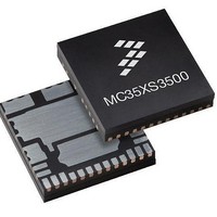
MC35XS3500PNA Freescale Semiconductor, MC35XS3500PNA Datasheet - Page 13

MC35XS3500PNA
Manufacturer Part Number
MC35XS3500PNA
Description
IC SWITCH HIGHSIDE 24PQFN
Manufacturer
Freescale Semiconductor
Type
High Side Switchr
Datasheet
1.MC35XS3500PNAR2.pdf
(41 pages)
Specifications of MC35XS3500PNA
Number Of Outputs
5
Rds (on)
*
Internal Switch(s)
Yes
Current Limit
9A
Voltage - Input
7 V ~ 20 V
Operating Temperature
-40°C ~ 125°C
Mounting Type
Surface Mount
Package / Case
24-PQFN, 24-PowerQFN
Product
MOSFET Gate Drivers
Rise Time
50 ns
Fall Time
50 ns
Propagation Delay Time
6.5 ms
Supply Voltage (max)
+ 5.5 V
Supply Voltage (min)
- 0.3 V
Supply Current
20 mA
Maximum Operating Temperature
+ 125
Minimum Operating Temperature
- 40 C
Lead Free Status / RoHS Status
Lead free / RoHS Compliant
Available stocks
Company
Part Number
Manufacturer
Quantity
Price
Analog Integrated Circuit Device Data
Freescale Semiconductor
Table 4. Dynamic Electrical Characteristics
Characteristics noted under conditions 4.5V
Typical values noted reflect the approximate parameter mean at T
POWER OUTPUTS TIMING (OUT1:5)
PWM MODULE
Notes
Current Sense Valid Time on resistive load only
Current Sense Synchronization Time on FETOUT
Current Sense Settling Time on resistive load only
Driver Output Positive Slew Rate (30% to 70% @ V
Driver Output Negative Slew Rate (70% to 30% @ V
Driver Output Matching Slew Rate (SR
@ 25 °C)
Driver Output Turn-ON Delay (SPI ON Command [No PWM,
Edge] to Output = 50% V
Driver Output Turn-OFF Delay (SPI OFF command [
Output = 50% V
Driver Output Matching Time (
with V
Nominal PWM Frequency Range
Clock Input Frequency Range
Output PWM Duty Cycle maximum range for 11 V<V
Output PWM Duty Cycle linear range for 11 V<V
Output PWM Duty Cycle range for full diagnostic for 11 V<VBAT<18 V
36.
37.
38.
39.
SR bit = 0, I
SR bit = 1, I
SR bit = 0, I
SR bit = 1, I
SR bit = 0, I
SR bit = 0, I
SR bit = 1, I
SR bit = 1, I
SR bit = 0
SR bit = 1
SR bit = 0
SR bit = 1
200 Hz Output PWM frequency
400 Hz Output PWM frequency
BAT
The PWM ratio is measured at V
cycle = 100%) and fully off (PWN duty cycle = 0%). Between 4%-96%, OCLO
Input Timing Switching Characteristics on page
Linear range is defined by output duty cycle to SPI duty cycle configuration +/- LSB. For values outside the linear duty cycle range, a
calibration curve is available.
Not production tested.
Full diagnositic corresponds to the availability of the following features: output current sensing, output status and openload detection.
Not production tested.
= 14 V, f
OUT
OUT
OUT
OUT
OUT
OUT
OUT
OUT
BAT
PWM
= 2.8 A
= 0.7 A
= 2.8 A
= 0.7 A
= 2.8 A
= 2.8 A
= 0.7 A
= 0.7 A
@ V
= 240 Hz, δ
BAT
BAT =
Characteristic
t
@ V
DLY(ON)
14 V)
(38)
BAT
PWM
R
= 14 V)
-
OUT
/SR
DYNAMIC ELECTRICAL CHARACTERISTICS
t
= 50%, @ 25 °C
DLY(OFF)
F
= 50% of V
)(70% to 30% @ V
(38)
BAT
≤
) @ Output = 50% V
(38)
V
BAT
<18 V
CC
CS
BAT
BAT
16.
BAT
= 14 V)
Positive Edge] to
≤
<18 V
= 14 V)
5.5V, 7.0V
(37), (38)
in nominal range of frequency. It is possible to put the device fully on (PWM duty
CS
(36), (38)
BAT
Positive
= 14 V
BAT
(39)
≤
V
A
BAT
= 25 °Χ under nominal conditions, unless otherwise noted.
t
PWM_MAX
t
t
≤
CSNS(SYNC)
PWM_DIAG
PWM_LIN
CSNS(VAL)
CSNS(SET)
t
Symbol
t
20V, -40 °Χ
DLYOFF
DLYON
f
Δ
SR
Δ SR
f
SR
PWM
CLK
t
1,2
RF
R
F
, OCLO and open load are available in ON state. See
DYNAMIC ELECTRICAL CHARACTERISTICS
≤
T
0.10
0.20
0.10
0.20
7.68
A
Min
- 30
0.8
4.0
5.5
5.5
50
25
50
25
30
11
–
–
–
–
–
≤
125 °Χ, unless otherwise noted.
ELECTRICAL CHARACTERISTICS
0.25
0.40
0.25
0.40
Typ
130
1.0
90
45
70
10
–
–
–
–
–
–
–
–
–
–
–
Max
0.56
0.80
0.56
0.80
51.2
150
185
110
120
120
400
1.2
75
30
65
65
30
96
96
96
90
35XS3500
V/μs
V/μs
Unit
kHz
Hz
μs
μs
μs
μs
μs
μs
%
%
%
13


