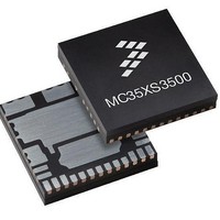
MC35XS3500PNA Freescale Semiconductor, MC35XS3500PNA Datasheet - Page 25

MC35XS3500PNA
Manufacturer Part Number
MC35XS3500PNA
Description
IC SWITCH HIGHSIDE 24PQFN
Manufacturer
Freescale Semiconductor
Type
High Side Switchr
Datasheet
1.MC35XS3500PNAR2.pdf
(41 pages)
Specifications of MC35XS3500PNA
Number Of Outputs
5
Rds (on)
*
Internal Switch(s)
Yes
Current Limit
9A
Voltage - Input
7 V ~ 20 V
Operating Temperature
-40°C ~ 125°C
Mounting Type
Surface Mount
Package / Case
24-PQFN, 24-PowerQFN
Product
MOSFET Gate Drivers
Rise Time
50 ns
Fall Time
50 ns
Propagation Delay Time
6.5 ms
Supply Voltage (max)
+ 5.5 V
Supply Voltage (min)
- 0.3 V
Supply Current
20 mA
Maximum Operating Temperature
+ 125
Minimum Operating Temperature
- 40 C
Lead Free Status / RoHS Status
Lead free / RoHS Compliant
Available stocks
Company
Part Number
Manufacturer
Quantity
Price
Serial Input Communication
accomplished using 16-bit messages. A message is
transmitted by the master starting with the MSB, D15, and
ending with the LSB, D0. Each incoming command message
on the SI pin can be interpreted using the bit assignment
described in
address bits, are used to select the command register. Bit
D10 is the watchdog bit. The remaining 10 bits, D9 : D0, are
used to configure and control the output and its protection
features. Multiple messages can be transmitted in
succession to accommodate those applications where daisy
chaining is desirable or to confirm transmitted data as long as
the messages are all multiples of 16 bits. Any attempt made
to latch in a message that is not 16 bits will be ignored.
equals 0 or fail mode (Fail=1).
ADDRESS
Initialization
Note: testmode address used only by FSL is D[15:11]=01111 with RST voltage higher than 8V typ.
Analog Integrated Circuit Device Data
Freescale Semiconductor
SI Register
Config OL
Config SR
Prescaler
External
SPI communication compliant to 3.3 V and 5.0 V is
All SPI registers are reset (all bits equal 0) in case of RST
Control
Control
Control
Control
Control
Control
The Initialization register is used to read the various
RESET
Config
Config
Switch
CSNS
OUT1
OUT2
OUT3
OUT4
OUT5
Table
D15 D14 D13 D12 D11 D10
00000 — Initialization
X
0
0
0
0
0
0
0
0
0
0
0
SI Address
X
0
0
0
0
0
1
1
1
1
1
1
7. The 5 bits D15 : D11, called register
X
0
0
0
0
0
0
0
0
1
1
1
X
0
0
1
1
1
0
1
1
0
0
1
Table 8. Serial Input Address and Configuration Bit Map
X
0
1
0
0
1
1
0
1
0
1
0
WD
WD
WD
WD
WD
WD Phase2 Phase1
WD Phase2 Phase1
WD Phase2 Phase1
WD Phase2 Phase1
WD Phase2 Phase1
WD Phase2 Phase1
0
LOGIC COMMANDS AND REGISTERS
Control5
CSNS
LED
sync
D9
0
0
1
0
Control4
LED
PR1
SR1
D8
0
0
0
STOPen
Control3
ONoff
ONoff
ONoff
ONoff
ONoff
ONoff
LED
PR2
SR2
D7
0
0
Device Register Addressing
serial input registers on device operation are described in this
section.
statuses, choose one of the six outputs current recopy,
enable the STOP pin, and synchronize the switching phases
Bit Sig
Control2
PWM6 PWM5 PWM4
PWM6 PWM5 PWM4
PWM6 PWM5 PWM4
PWM6 PWM5 PWM4
PWM6 PWM5 PWM4
PWM6 PWM5 PWM4
MSB
PWM
LSB
sync
LED
PR3
SR3
D6
The register addresses (D15 : D11) and the impact of the
0
0
Control1
Table 8
SI Msg Bit
SI Data
LED
D15 : D11
D5
0
0
0
0
0
Table 7. SI Message Bit Assignment
D9 : D0
D10
OLLED
NO_OCHI5
MUX2
summarizes the content of the SI registers.
D4
5
0
0
0
Register address bits.
Watchdog in: toggled to satisfy watchdog
requirements.
Used to configure inputs, outputs, device
protection features, and SO status content.
LOGIC COMMANDS AND REGISTERS
OLLED
NO_OCHI4
PWM3
PWM3
PWM3
PWM3
PWM3
PWM3
MUX1
D3
FUNCTIONAL DEVICE OPERATION
4
0
0
0
Message Bit Description
OLLED
NO_OCHI3
PWM2
PWM2
PWM2
PWM2
PWM2
PWM2
MUX0
PR4
SR4
D2
3
0
OLLED
NO_OCHI2
PWM1
PWM1
PWM1
PWM1
PWM1
PWM1
SOA1
PR5
SR5
D1
2
0
OLLED
NO_OCHI1
PWM0
PWM0
PWM0
PWM0
PWM0
PWM0
SOA0
PR6
D0
35XS3500
1
0
0
25


