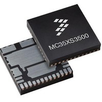
MC35XS3500PNA Freescale Semiconductor, MC35XS3500PNA Datasheet - Page 21

MC35XS3500PNA
Manufacturer Part Number
MC35XS3500PNA
Description
IC SWITCH HIGHSIDE 24PQFN
Manufacturer
Freescale Semiconductor
Type
High Side Switchr
Datasheet
1.MC35XS3500PNAR2.pdf
(41 pages)
Specifications of MC35XS3500PNA
Number Of Outputs
5
Rds (on)
*
Internal Switch(s)
Yes
Current Limit
9A
Voltage - Input
7 V ~ 20 V
Operating Temperature
-40°C ~ 125°C
Mounting Type
Surface Mount
Package / Case
24-PQFN, 24-PowerQFN
Product
MOSFET Gate Drivers
Rise Time
50 ns
Fall Time
50 ns
Propagation Delay Time
6.5 ms
Supply Voltage (max)
+ 5.5 V
Supply Voltage (min)
- 0.3 V
Supply Current
20 mA
Maximum Operating Temperature
+ 125
Minimum Operating Temperature
- 40 C
Lead Free Status / RoHS Status
Lead free / RoHS Compliant
Available stocks
Company
Part Number
Manufacturer
Quantity
Price
Sleep Mode
This is the state of the device after first applying battery
voltage (V
state of the device when IGN, RST, FLASHER, and STOP
are logic [0]. In the Sleep mode, the output and all internal
circuitry are OFF to minimize current draw. In addition, all
SPI-configurable features of the device are reset. The
35XS3500 will transit to two modes (Normal and Fail)
depending on wake and fail signals (see
window).
following signals:
control of the SPI as follows:
current behavior in Normal mode.
Normal Mode
Analog Integrated Circuit Device Data
Freescale Semiconductor
The Sleep mode is the default mode of the 35XS3500.
The transition to the other modes is according to the
• Wake = IGN or IGN_ON or FLASHER or
• Fail = VCC fail or SPI fail or External limp
The 35XS3500 is in Normal mode when:
• Wake = 1
• Fail = 0
I
• The outputs 1 to 6, including multiphase timing, and
• The output 4 is activated directly by the STOP external
• The outputs 1 to 5 are switched OFF in case of under-
• The outputs 1 to 5 are protected by the selectable over-
• The digital diagnosis feature transfers status of the
• The analog current sense output (current recopy
• The outputs can be configured to control LED loads:
• The SPI reports NM=1 in this mode.
The following figure describes the PWM, outputs and over-
n Normal operating mode the power outputs are under full
FLASHER_ON or STOP or STOP_ON or RST
selectable slew-rate, are controlled by the
programmable PWM module.
pin in case the STOP_en bit is set to a logic [1].
voltage on VBAT.
current double window and over-temperature shutdown
circuit.
smart outputs via the SPI.
feature) can be rerouted by the SPI.
R
recopy ratio is scaled by a factor of 4.
DS(ON)
Tail Light
Output 1
IGN Pin
BAT
) and prior to any I /O transitions. This is also the
is increased by a factor of 2 and the current
License Light
Output 2
OFF
FUNCTIONAL DEVICE OPERATION
Table 18, Watchdog
Rear Drive Light
Table 6. Limp Home Output State
Output 3
OFF
OPERATIONAL MODES
Fail Mode
Stop Light
STOP Pin
Output 4
IGN_ON
The 35XS3500 is in Fail mode when:
• Wake = 1
• Fail = 1
In Fail mode:
• The outputs are under control of the external pins (see
• The outputs are fully protected in case of overload,
• The SPI reports continously the content of address 11,
• Neither digital diagnosis feature (SPI) nor analog
• In case of overload (OCHI2 or OCLO) conditions or
• In case of a serious overload condition (OCHI1 or OT)
IGN (external)
OUT[1,2]
Over-current
D7 bit
D0-D6 bits
Output
Over-current
Table 5).
over-temperature and under-voltage (on B
V
disregard to previous requested output data word.
current sense are available.
under-voltage on VBAT, the outputs are under control
of the autorestart feature.
the corresponding output is latched OFF until a new
wake-up event (wake = 0 then 1)
CC
).
FLASHER Pin
Output 5
Flasher
FUNCTIONAL DEVICE OPERATION
1.4 sec min
OPERATIONAL MODES
External Switch
Rear Fog Light
OFF
VAT
35XS3500
or on
21


