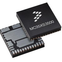
MC35XS3500PNA Freescale Semiconductor, MC35XS3500PNA Datasheet - Page 20

MC35XS3500PNA
Manufacturer Part Number
MC35XS3500PNA
Description
IC SWITCH HIGHSIDE 24PQFN
Manufacturer
Freescale Semiconductor
Type
High Side Switchr
Datasheet
1.MC35XS3500PNAR2.pdf
(41 pages)
Specifications of MC35XS3500PNA
Number Of Outputs
5
Rds (on)
*
Internal Switch(s)
Yes
Current Limit
9A
Voltage - Input
7 V ~ 20 V
Operating Temperature
-40°C ~ 125°C
Mounting Type
Surface Mount
Package / Case
24-PQFN, 24-PowerQFN
Product
MOSFET Gate Drivers
Rise Time
50 ns
Fall Time
50 ns
Propagation Delay Time
6.5 ms
Supply Voltage (max)
+ 5.5 V
Supply Voltage (min)
- 0.3 V
Supply Current
20 mA
Maximum Operating Temperature
+ 125
Minimum Operating Temperature
- 40 C
Lead Free Status / RoHS Status
Lead free / RoHS Compliant
Available stocks
Company
Part Number
Manufacturer
Quantity
Price
Serial Input (SI)
Each SI bit is read on the falling edge of SCLK. A 16-bit
stream of serial data is required on the SI pin, starting with
D15 to D0. SI has a passive pull-down, R
Serial Output (SO)
The SO pin remains in a high-impedance state until the CS
pin is put into a logic [0] state. The SO data is capable of
reporting the status of the output, the device configuration,
and the state of the key inputs. The SO pin changes state on
the rising edge of SCLK and reads out on the falling edge of
SCLK.
20
35XS350
FUNCTIONAL DESCRIPTION
FUNCTIONAL PIN DESCRIPTION
The SI pin is a serial interface command data input pin.
The SO data pin is a tri-state output from the shift register.
CSB
SCLK
CS
SO
SI
NOTES:
Notes
D15
1.
2.
3
OD15
1. D15:D0 relate to the most recent ordered entry of data into the device.
2. OD15:OD0 relate to the first 16 bits of ordered fault and status data out of the device.
RSTB is in a logic H state during the above operation.
DO, D1, D2, ... , and D15 relate to the most recent ordered entry of program data into the LUX IC
OD0 OD1 OD2
D14
OD14
D13
OD13
D12
OD12
and OD15 relate to the first 16 bits of ordered fault and status data out of the LUX IC
Figure 8. Single 16-Bit Word SPI Communication
D11
OD11
DOWN
CS
D10
.
OD10
D9
OD9
D8
OD8
D7
OD7
Chip Select (CS)
device. When this pin is in a logic [0] state, the device is
capable of transferring information to, and receiving
information from, the master device. The 35XS3500 device
latches in data from the Input Shift registers to the addressed
registers on the rising edge of CS. The device transfers
status information from the power output to the Shift register
on the falling edge of CS. The SO output driver is enabled
when CS is logic [0]. CS should transition from a logic [1] to a
logic [0] state only when SCLK is a logic [0]. CS has a
passive pull-up, R
STOP Input (STOP)
mode activation. The signal is “high active“, meaning the
component is active in case of a logic high at the input.
The CS pin enables communication with the master
The STOP input wakes the device. It also controls the Fail
D6
OD6
D5
OD5
D4
OD4
UP
.
device.
Analog Integrated Circuit Device Data
D3
OD3
device.
D2
OD2
Freescale Semiconductor
D1
OD1
D0
OD0


