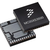
MC35XS3500PNA Freescale Semiconductor, MC35XS3500PNA Datasheet - Page 3

MC35XS3500PNA
Manufacturer Part Number
MC35XS3500PNA
Description
IC SWITCH HIGHSIDE 24PQFN
Manufacturer
Freescale Semiconductor
Type
High Side Switchr
Datasheet
1.MC35XS3500PNAR2.pdf
(41 pages)
Specifications of MC35XS3500PNA
Number Of Outputs
5
Rds (on)
*
Internal Switch(s)
Yes
Current Limit
9A
Voltage - Input
7 V ~ 20 V
Operating Temperature
-40°C ~ 125°C
Mounting Type
Surface Mount
Package / Case
24-PQFN, 24-PowerQFN
Product
MOSFET Gate Drivers
Rise Time
50 ns
Fall Time
50 ns
Propagation Delay Time
6.5 ms
Supply Voltage (max)
+ 5.5 V
Supply Voltage (min)
- 0.3 V
Supply Current
20 mA
Maximum Operating Temperature
+ 125
Minimum Operating Temperature
- 40 C
Lead Free Status / RoHS Status
Lead free / RoHS Compliant
Available stocks
Company
Part Number
Manufacturer
Quantity
Price
Table 1. 35XS3500 Pin Definitions
Analog Integrated Circuit Device Data
Freescale Semiconductor
Functional descriptions these pins can be found in the
Pin
1
2
3
4
5
6
7
8
9
FLASHER
Pin Name
CLOCK
FETIN
STOP
SCLK
LIMP
RST
IGN
CS
Figure 3. 35XS3500 Pin Connections (Transparent Package Top View)
Pin Function
Input
Input
Input
Input
Input
Input
Input
Input
Input
OUT5
GND
CP
13
External FET Input
16
17
18
Limp Home Input
Stop Light Input
SPI Clock Input
Formal Name
12
Ignition Input
(Active High)
Flasher Input
(Active High)
(Active High)
(Active High)
OUT4
(Active Low)
Chip Select
Clock Input
19
Reset
11
PIN CONNECTIONS
10
9
Functional Description
8
VBAT
This pin is the current sense recopy of the external MOSFET.
This input wakes the device. It also controls outputs 1 and 2 in case of Fail
mode activation. This pin has a passive internal pull-down.
This input wakes the device. It is also used to initialize the device
configuration and fault registers through the SPI. This pin has a passive
internal pull-down.
This input wakes the device. This pin has a passive internal pull-down.
This pin state depends on RST logic level.
As long as RST input pin is set to logic [0], this pin is pulled up in order to
report wake event. Otherwise, the PWM frequency and timing are
generated from this digital clock input by the PWM module.
This pin has a passive internal pull-down.
The Fail mode can be activated by this digital input. This pin has an active
internal pull-down current source.
This input wakes the device. This pin has a passive internal pull-down.
When this signal is high, SPI signals are ignored. Asserting this pin low
starts a SPI transaction. The transaction is signaled as completed when
this signal returns high. This pin has a passice internal pull-up resistance.
This input pin is connected to the master microcontroller providing the
required bit shift clock for SPI communication. This pin has a passive
internal pull-down resistance.
GND
OUT3
14
15
20
7
6
5
4
3
OUT2
section beginning on
21
2
24
23
22
1
Definition
CSNS
GND
OUT1
page
PIN CONNECTIONS
18.
35XS3500
3


