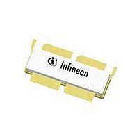
PTFB213004F V1 Infineon Technologies, PTFB213004F V1 Datasheet - Page 2

PTFB213004F V1
Manufacturer Part Number
PTFB213004F V1
Description
RF MOSFET Small Signal RFP-LDMOS 9
Manufacturer
Infineon Technologies
Datasheet
1.PTFB213004F_V2.pdf
(16 pages)
Specifications of PTFB213004F V1
Configuration
Single
Resistance Drain-source Rds (on)
0.03 Ohms
Drain-source Breakdown Voltage
65 V
Gate-source Breakdown Voltage
10 V
Continuous Drain Current
2.4 A
Maximum Operating Temperature
+ 125 C
Minimum Operating Temperature
- 40 C
Package / Case
H-37275-6
Other names
FB213004FV1NP
Confidential, Limited Internal Distribution
RF Characteristics
Two-tone Measurements
V
Characteristic
Gain
Drain Efficiency
Intermodulation Distortion
DC Characteristics
Characteristic
Drain-Source Breakdown Voltage
Drain Leakage Current
On-State Resistance
Operating Gate Voltage
Gate Leakage Current
Maximum Ratings
Parameter
Drain-Source Voltage
Gate-Source Voltage
Junction Temperature
Storage Temperature Range
Thermal Resistance (T
Ordering Information
Type and Version
PTFB213004F V2
PTFB213004F V2 R250 H-37275-6/2
Data Sheet
DD
= 30 V, I
DQ
= 2.4 A, P
CASE
Package Outline
H-37275-6/2
OUT
(cont.)
= 70°C )
(not subject to production test—verified by design / characterization in Infineon test fixture)
= 250 W PEP, ƒ = 2140 MHz, tone spacing = 1 MHz
Conditions
V
V
V
V
V
V
GS
DS
DS
GS
DS
GS
= 0 V, I
= 30 V, V
= 63 V, V
= 10 V, V
= 30 V, I
= 10 V, V
DS
DQ
GS
GS
Package Description
Thermally-enhanced earless flange
Thermally-enhanced earless flange
DS
DS
= 10 µA
= 2.4 A
= 0 V
= 0 V
= 0.1 A
= 0 V
2 of 16
V
Symbol
Symbol
Symbol
R
(BR)DSS
V
T
R
I
I
I
DS(on)
V
V
G
IMD
DSS
DSS
GSS
hD
DSS
STG
T
qJC
GS
GS
ps
J
Min
Min
2.3
65
—
—
—
—
—
—
—
–40 to +150
–0.5 to +65
–6 to +10
Value
Typ
Typ
0.03
0.23
–30
200
2.8
18
37
—
—
—
—
Shipping
Tray
Tape & Reel
PTFB213004F
Rev. 05.2, 2010-12-09
Max
Max
10.0
1.0
3.3
1.0
—
—
—
—
—
°C/W
Unit
Unit
Unit
dBc
dB
µA
µA
µA
°C
°C
%
W
V
V
V
V


