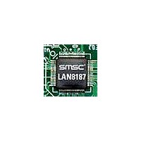
LAN8187-JT SMSC, LAN8187-JT Datasheet - Page 16

LAN8187-JT
Manufacturer Part Number
LAN8187-JT
Description
Ethernet ICs HiPerfrm Ethrnt PHY
Manufacturer
SMSC
Type
MII/RMII Ethernet Transceiverr
Datasheet
1.LAN8187-JT.pdf
(78 pages)
Specifications of LAN8187-JT
Ethernet Connection Type
10 Base-T, 100 Base-TX
Minimum Operating Temperature
0 C
Mounting Style
SMD/SMT
Product
Ethernet Transceivers
Number Of Transceivers
1
Standard Supported
802.3ab
Data Rate
10 MB, 100 MB
Supply Voltage (max)
3.3 V
Supply Voltage (min)
1.8 V
Supply Current (max)
39 mA, 81.6 mA
Maximum Operating Temperature
+ 70 C
Package / Case
TQFP-64
Lead Free Status / RoHS Status
Lead free / RoHS Compliant
Available stocks
Company
Part Number
Manufacturer
Quantity
Price
Company:
Part Number:
LAN8187-JT
Manufacturer:
Standard
Quantity:
1 040
Company:
Part Number:
LAN8187-JT
Manufacturer:
STM
Quantity:
5 362
Part Number:
LAN8187-JT
Manufacturer:
SMSC
Quantity:
20 000
Revision 1.7 (03-04-11)
SIGNAL NAME
SIGNAL NAME
CLKIN/XTAL1
GPO0/RMII
XTAL2
GPO2
GPO1
nRST
nINT
TXN
TXP
TYPE
TYPE
AO
AO
I/O
I/O
Table 3.6 10/100 Line Interface
O
O
O
I
I
Table 3.5 General Signals
±15kV ESD Protected MII/RMII 10/100 Ethernet Transceiver with HP Auto-MDIX & flexPWR
DATASHEET
LAN Interrupt – Active Low output. Place a pull-up external
resistor (see
on page
Notes:
External Reset – input of the system reset. This signal is active
LOW. When this pin is deasserted, the mode register bits are
loaded from the mode pins as described in
Clock Input – 25 Mhz or 50 MHz external clock or crystal input.
In MII mode, this signal is the 25 MHz reference input clock
In RMII mode, this signal is the 50 MHz reference input clock
which is typically also driven to the RMII compliant Ethernet MAC
clock input.
Note:
Clock Output – 25 MHz crystal output.
Note:
General Purpose Output 2 – General Purpose Output signal
Driven by bits in registers 27 and 31.
General Purpose Output 1 – General Purpose Output signal
Driven by bits in registers 27 and 31. This signal is mux’d with
PHYAD4.
General Purpose Output 0 – General Purpose Output signal.
Driven by bits in registers 27 and 31.
RMII – MII/RMII mode selection is latched on the rising edge of
nRST based on the following strapping:
Float the GPO0 pin for MII mode or pull-high with an external
resistor to VDDIO to set the device in RMII mode. See
“Boot Strapping Configuration Resistors,” on page 33
Note:
Transmit Data: 100Base-TX or 10Base-T differential transmit
outputs to magnetics.
Transmit Data: 100Base-TX or 10Base-T differential transmit
outputs to magnetics.
This signal is mux’d with TX_ER/TXD4
See
page 32
Section 4.10, "(TX_ER/TXD4)/nINT Strapping," on
16
33) to VCC 3.3V.
See
page 32
See
page 32
Also, float this pin if using an external clock being
driven through CLKIN/XTAL1
See
page 26
for additional details on Strapping options.
Table 4.4, “Boot Strapping Configuration Resistors,”
Section 4.10, "(TX_ER/TXD4)/nINT Strapping," on
Section 4.10, "(TX_ER/TXD4)/nINT Strapping," on
Section 4.6.3, "MII vs. RMII Configuration," on
for additional details on Strapping options.
for additional details on Strapping options.
for more details.
DESCRIPTION
DESCRIPTION
SMSC LAN8187/LAN8187i
Section
5.4.9.2.
Table 4.4,
Datasheet
®
Technology


