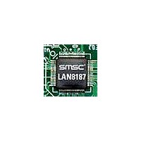
LAN8187-JT SMSC, LAN8187-JT Datasheet - Page 32

LAN8187-JT
Manufacturer Part Number
LAN8187-JT
Description
Ethernet ICs HiPerfrm Ethrnt PHY
Manufacturer
SMSC
Type
MII/RMII Ethernet Transceiverr
Datasheet
1.LAN8187-JT.pdf
(78 pages)
Specifications of LAN8187-JT
Ethernet Connection Type
10 Base-T, 100 Base-TX
Minimum Operating Temperature
0 C
Mounting Style
SMD/SMT
Product
Ethernet Transceivers
Number Of Transceivers
1
Standard Supported
802.3ab
Data Rate
10 MB, 100 MB
Supply Voltage (max)
3.3 V
Supply Voltage (min)
1.8 V
Supply Current (max)
39 mA, 81.6 mA
Maximum Operating Temperature
+ 70 C
Package / Case
TQFP-64
Lead Free Status / RoHS Status
Lead free / RoHS Compliant
Available stocks
Company
Part Number
Manufacturer
Quantity
Price
Company:
Part Number:
LAN8187-JT
Manufacturer:
Standard
Quantity:
1 040
Company:
Part Number:
LAN8187-JT
Manufacturer:
STM
Quantity:
5 362
Part Number:
LAN8187-JT
Manufacturer:
SMSC
Quantity:
20 000
Revision 1.7 (03-04-11)
4.10
4.11
4.12
4.12.1
LED output = active low
The TX_ER, TXD4 and nINT functions share a common pin. There are two functional modes for this
pin, the TX_ER/TXD4 mode and nINT (interrupt) mode. The RXD3 pin is used to select one of these
two functional modes.
The RXD3 pin is latched on the rising edge of the internal reset (nreset) to select the mode. The
system designer must float the RXD3 pin for nINT mode or pull-low with an external resistor (see
Table 4.4, “Boot Strapping Configuration Resistors,” on page
TX_ER/TXD4 mode. The default setting is high (nINT mode).
The PHY ADDRESS bits are latched on the rising edge of the internal reset (nreset). The 5-bit address
word[0:4] is input on the LED1, LED2, LED3, LED4, GPO1 output pins. The default setting is all high
5'b1_1111.
The address lines are strapped as defined in the diagram below. The LED outputs will automatically
change polarity based on the presence of an external pull-down resistor. If the LED pin is pulled high
(by an internal 100K pull-up resistor) to select a logical high PHY address, then the LED output will
be active low. If the LED pin is pulled low (by an external pull-down resistor (see
Strapping Configuration Resistors,” on page
will then be an active high output.
To set the PHY address on the LED pins without LEDs or on the GPO1 or CRS pin, float the pin to
set the address high or pull-down the pin with an external resistor (see
Configuration Resistors,” on page
The Digital I/O pins on the LAN8187/LAN8187i are variable voltage to take advantage of low power
savings from shrinking technologies. These pins can operate from a low I/O voltage of +1.6V up to
+3.6V. Due to this low voltage feature addition, the system designer needs to take consideration as
for two aspects of their design. Boot strapping configuration and I/O voltage stability.
Boot Strapping Configuration
Due to a lower I/O voltage, a lower strapping resistor needs to be used to ensure the strapped
configuration is latched into the PHY device at power-on reset.
(TX_ER/TXD4)/nINT Strapping
PHY Address Strapping and LED Output Polarity Selection
Variable Voltage I/O
Phy Address = 1
VDDIO
~270 ohms
Figure 4.5 PHY Address Strapping on LED’s
LED1-LED4
±15kV ESD Protected MII/RMII 10/100 Ethernet Transceiver with HP Auto-MDIX & flexPWR
~10K ohms
33) to GND to set the address low. See the figure below:
DATASHEET
32
LED output = active high
33) to select a logical low PHY address, the LED output
Phy Address = 0
~270 ohms
33) to VSS to set the device in
LED1-LED4
Table 4.4, “Boot Strapping
SMSC LAN8187/LAN8187i
Table 4.4, “Boot
Datasheet
®
Technology


