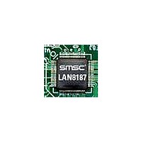
LAN8187-JT SMSC, LAN8187-JT Datasheet - Page 25

LAN8187-JT
Manufacturer Part Number
LAN8187-JT
Description
Ethernet ICs HiPerfrm Ethrnt PHY
Manufacturer
SMSC
Type
MII/RMII Ethernet Transceiverr
Datasheet
1.LAN8187-JT.pdf
(78 pages)
Specifications of LAN8187-JT
Ethernet Connection Type
10 Base-T, 100 Base-TX
Minimum Operating Temperature
0 C
Mounting Style
SMD/SMT
Product
Ethernet Transceivers
Number Of Transceivers
1
Standard Supported
802.3ab
Data Rate
10 MB, 100 MB
Supply Voltage (max)
3.3 V
Supply Voltage (min)
1.8 V
Supply Current (max)
39 mA, 81.6 mA
Maximum Operating Temperature
+ 70 C
Package / Case
TQFP-64
Lead Free Status / RoHS Status
Lead free / RoHS Compliant
Available stocks
Company
Part Number
Manufacturer
Quantity
Price
Company:
Part Number:
LAN8187-JT
Manufacturer:
Standard
Quantity:
1 040
Company:
Part Number:
LAN8187-JT
Manufacturer:
STM
Quantity:
5 362
Part Number:
LAN8187-JT
Manufacturer:
SMSC
Quantity:
20 000
±15kV ESD Protected MII/RMII 10/100 Ethernet Transceiver with HP Auto-MDIX & flexPWR
Datasheet
SMSC LAN8187/LAN8187i
4.5.4
4.6
4.6.1
4.6.2
Jabber Detection
Jabber is a condition in which a station transmits for a period of time longer than the maximum
permissible packet length, usually due to a fault condition, that results in holding the TX_EN input for
a long period. Special logic is used to detect the jabber state and abort the transmission to the line,
within 45ms. Once TX_EN is deasserted, the logic resets the jabber condition.
As shown in
The MII/RMII block is responsible for the communication with the controller. Special sets of hand-shake
signals are used to indicate that valid received/transmitted data is present on the 4 bit receive/transmit
bus.
The device must be configured in MII or RMII mode. This is done by specific pin strapping
configurations.
See section
and how the pins are mapped differently.
MII
The MII includes 16 interface signals:
In MII mode, on the transmit path, the PHY drives the transmit clock, TX_CLK, to the controller. The
controller synchronizes the transmit data to the rising edge of TX_CLK. The controller drives TX_EN
high to indicate valid transmit data. The controller drives TX_ER high when a transmit error is detected.
On the receive path, the PHY drives both the receive data, RXD[3:0], and the RX_CLK signal. The
controller clocks in the receive data on the rising edge of RX_CLK when the PHY drives RX_DV high.
The PHY drives RX_ER high when a receive error is detected.
RMII
The SMSC LAN8187/LAN8187i supports the low pin count Reduced Media Independent Interface
(RMII) intended for use between Ethernet PHYs and Switch ASICs. Under IEEE 802.3, an MII
comprised of 16 pins for data and control is defined. In devices incorporating many MACs or PHY
interfaces such as switches, the number of pins can add significant cost as the port counts increase.
The management interface (MDIO/MDC) is identical to MII. The RMII interface has the following
characteristics:
MAC Interface
transmit data - TXD[3:0]
transmit strobe - TX_EN
transmit clock - TX_CLK
transmit error - TX_ER/TXD4
receive data - RXD[3:0]
receive strobe - RX_DV
receive clock - RX_CLK
receive error - RX_ER/RXD4
collision indication - COL
carrier sense - CRS
It is capable of supporting 10Mb/s and 100Mb/s data rates
A single clock reference is sourced from the MAC to PHY (or from an external source)
It provides independent 2 bit wide (di-bit) transmit and receive data paths
Section 4.6.3, "MII vs. RMII Configuration," on page 26
Table
5.31, bit 1.1 indicates that a jabber condition was detected.
DATASHEET
25
®
Technology
for information on pin strapping
Revision 1.7 (03-04-11)


