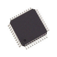
82V2041EPPG IDT, Integrated Device Technology Inc, 82V2041EPPG Datasheet - Page 11

82V2041EPPG
Manufacturer Part Number
82V2041EPPG
Description
Manufacturer
IDT, Integrated Device Technology Inc
Datasheet
1.82V2041EPPG.pdf
(75 pages)
Specifications of 82V2041EPPG
Number Of Transceivers
1
Screening Level
Industrial
Mounting
Surface Mount
Package Type
TQFP
Operating Temperature (min)
-40C
Operating Temperature (max)
85C
Lead Free Status / RoHS Status
Compliant
Table-1 Pin Description (Continued)
Pin Description
IDT82V2041E
RXTXM1
RXTXM0
Name
SCLK
ALE
R/W
LP1
LP0
INT
SDI
WR
CS
AS
Type
O
I
I
I
I
Pin No.
21
20
25
24
CS: Chip Select
In serial or parallel microcontroller interface mode, this is the active low enable signal. A low level on this pin enables serial or
parallel microcontroller interface.
RXTXM[1:0]: Receive and transmit path operation mode select
In hardware control mode, these pins are used to select the single rail or dual rail operation modes as well as AMI or HDB3/
B8ZS line coding:
•
•
•
•
INT: Interrupt Request
In software control mode, this pin outputs the general interrupt request for all interrupt sources. These interrupt sources can be
masked individually via registers (INTM0, 14H) and (INTM1, 15H). The interrupt status is reported via the registers (INTS0,
19H) and (INTS1, 1AH).
Output characteristics of this pin can be defined to be push-pull (active high or active low) or open-drain (active low) by setting
INT_PIN[1:0] (GCF, 02H).
RXTXM0
See RXTXM1 above.
SCLK: Shift Clock
In serial microcontroller interface mode, this signal is the shift clock for the serial interface. Configuration data on SDI pin is sam-
pled on the rising edge of SCLK. Configuration and status data on SDO pin is clocked out of the device on the falling edge of
SCLK if SCLKE pin is high, or on the rising edge of SCLK if SCLKE pin is low.
ALE: Address Latch Enable
In parallel microcontroller interface mode with multiplexed Intel interface, the address on AD[7:0] is sampled into the device on
the falling edge of ALE.
AS: Address Strobe
In parallel microcontroller interface mode with multiplexed Motorola interface, the address on AD[7:0] is latched into the device
on the falling edge of AS.
LP[1:0]: Loopback mode select
When the chip is configured by hardware, this pin is used to select loopback operation modes (Inband Loopback is not provided
in hardware control mode):
•
•
•
•
SDI: Serial Data Input
In serial microcontroller interface mode, this signal is the input data to the serial interface. Configuration data at SDI pin is sam-
pled by the device on the rising edge of SCLK.
WR: Write Strobe
In Intel parallel multiplexed interface mode, this pin is asserted low by the microcontroller to initiate a write cycle. The data on
AD[7:0] is sampled into the device in a write operation.
R/W: Read/Write Select
In Motorola parallel multiplexed interface mode, this pin is low for write operation and high for read operation.
LP0
See LP1 above.
00= single rail with HDB3/B8ZS coding
01= single rail with AMI coding
10= dual rail interface with CDR enabled
11= slicer mode (dual rail interface with CDR disabled)
00= no loopback
01= analog loopback
10= digital loopback
11= remote loopback
SINGLE CHANNEL T1/E1/J1 SHORT HAUL LINE INTERFACE UNIT
11
Description
December 9, 2005


