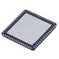
AD9548BCPZ Analog Devices Inc, AD9548BCPZ Datasheet - Page 16

AD9548BCPZ
Manufacturer Part Number
AD9548BCPZ
Description
IC CLOCK GEN/SYNCHRONIZR 88LFCSP
Manufacturer
Analog Devices Inc
Datasheet
1.AD9548BCPZ-REEL7.pdf
(112 pages)
Specifications of AD9548BCPZ
Input
*
Output
*
Frequency - Max
*
Voltage - Supply
*
Operating Temperature
*
Mounting Type
Surface Mount
Package / Case
88-LFCSP
Frequency-max
*
Clock Ic Type
Clock Synthesizer
Ic Interface Type
Serial
Frequency
1GHz
No. Of Outputs
4
No. Of Multipliers / Dividers
4
Supply Current
190mA
Lead Free Status / RoHS Status
Lead free / RoHS Compliant
Available stocks
Company
Part Number
Manufacturer
Quantity
Price
Part Number:
AD9548BCPZ
Manufacturer:
ADI/亚德诺
Quantity:
20 000
Company:
Part Number:
AD9548BCPZ-SMD7
Manufacturer:
SHARP
Quantity:
392
AD9548
Pin No.
21, 22
23, 24
26
27
29
30
31, 37, 38,
44
32
33
34, 41
35
36
39
40
42
43
47
48
49
50, 55
52
Mnemonic
AVDD3
AVDD
CLKINN
CLKINP
AVDD
OUT_RSET
AVDD3
OUT0P
OUT0N
AVDD
OUT1P
OUT1N
OUT2P
OUT2N
OUT3P
OUT3N
AVDD3
SYSCLK_VREG
SYSCLK_LF
AVDD
SYSCLKN
Input/
Output
I
I
I
I
I
O
I
O
O
I
O
O
O
O
O
O
I
I
O
I
I
Pin Type
Power
Power
Differential
input
Differential
input
Power
Current set
resistor
Power
LVPECL,
LVDS, or
CMOS
LVPECL,
LVDS, or
CMOS
Power
LVPECL,
LVDS, or
CMOS
LVPECL,
LVDS, or
CMOS
LVPECL,
LVDS, or
CMOS
LVPECL,
LVDS, or
CMOS
LVPECL,
LVDS, or
CMOS
LVPECL,
LVDS, or
CMOS
Power
Power
Differential
input
Description
3.3 V Analog (DAC) Power Supply.
1.8 V Analog (DAC) Power Supply.
Clock Distribution Input. In standard operating mode, this pin is connected to the
filtered DACOUTN output. This internally biased input is typically ac-coupled and,
when configured as such, can accept any differential signal whose single-ended
swing is at least 400 mV.
Clock Distribution Input. In standard operating mode, this pin is connected to the
filtered DACOUTP output
1.8 V Analog (Input Receiver) Power Supply.
Connect an optional 3.12 kΩ resistor from this pin to ground (see the Output
Current Control with an External Resistor section).
Analog Supply for Output Driver. These pins are normally 3.3 V but can be 1.8 V.
Pin 31 powers Out0x. Pin 37 powers OUT1x. Pin 38 powers OUT2x. Pin 44 powers
OUT3x. Apply power to these pins even if the corresponding outputs (OUT0P/
OUT0N, OUT1P/ OUT1N, OUT2P/ OUT2N, and OUT3P/ OUT3N) are not used. See
the Power Supply Partitions section.
Output 0. This output can be configured as LVPECL, LVDS, or single-ended CMOS.
LVPECL and LVDS operation require a 3.3 V output driver power supply. CMOS
operation can be either 1.8 V or 3.3 V, depending on the output driver power
supply.
Complementary Output 0. This output can be configured as LVPECL, LVDS, or
single-ended CMOS.
1.8 V Analog (Output Divider) Power Supply.
Output 1. This output can be configured as LVPECL, LVDS, or single-ended CMOS.
LVPECL and LVDS operation require a 3.3 V output driver power supply. CMOS
operation can be either 1.8 V or 3.3 V, depending on the output driver power
supply.
Complementary Output 1. This output can be configured as LVPECL, LVDS, or
single-ended CMOS.
Output 2. This output can be configured as LVPECL, LVDS, or single-ended CMOS.
LVPECL and LVDS operation require a 3.3 V output driver power supply. CMOS
operation can be either 1.8 V or 3.3 V, depending on the output driver power
supply.
Complementary Output 2. This output can be configured as LVPECL, LVDS, or
single-ended CMOS.
Output 3. This output can be configured as LVPECL, LVDS, or single-ended CMOS.
LVPECL and LVDS operation require a 3.3 V output driver power supply. CMOS
operation can be either 1.8 V or 3.3 V, depending on the output driver power
supply.
Complementary Output 3. This output can be configured as LVPECL, LVDS, or
single-ended CMOS.
3.3 V Analog (System Clock) Power Supply.
System Clock Loop Filter Voltage Regulator. Connect a 0.1 μF capacitor from this
pin to ground. This pin is also the ac ground reference for the integrated SYSCLK
PLL multiplier’s external loop filter (see the SYSCLK PLL Multiplier section).
System Clock Multiplier Loop Filter. When using the frequency multiplier to drive
the system clock, an external loop filter can be attached to this pin.
1.8 V Analog (System Clock) Power Supply.
Complementary System Clock Input. Complementary signal to SYSCLKP. SYSCLKN
contains internal dc biasing and should be ac-coupled with a 0.01 μF capacitor,
except when using a crystal, in which case connect the crystal across SYSCLKP
and SYSCLKN.
Rev. A | Page 16 of 112


