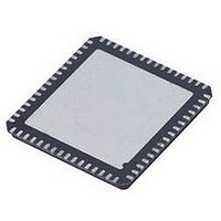
AD9548BCPZ Analog Devices Inc, AD9548BCPZ Datasheet - Page 70

AD9548BCPZ
Manufacturer Part Number
AD9548BCPZ
Description
IC CLOCK GEN/SYNCHRONIZR 88LFCSP
Manufacturer
Analog Devices Inc
Datasheet
1.AD9548BCPZ-REEL7.pdf
(112 pages)
Specifications of AD9548BCPZ
Input
*
Output
*
Frequency - Max
*
Voltage - Supply
*
Operating Temperature
*
Mounting Type
Surface Mount
Package / Case
88-LFCSP
Frequency-max
*
Clock Ic Type
Clock Synthesizer
Ic Interface Type
Serial
Frequency
1GHz
No. Of Outputs
4
No. Of Multipliers / Dividers
4
Supply Current
190mA
Lead Free Status / RoHS Status
Lead free / RoHS Compliant
Available stocks
Company
Part Number
Manufacturer
Quantity
Price
Part Number:
AD9548BCPZ
Manufacturer:
ADI/亚德诺
Quantity:
20 000
Company:
Part Number:
AD9548BCPZ-SMD7
Manufacturer:
SHARP
Quantity:
392
AD9548
REGISTER MAP BIT DESCRIPTIONS
SERIAL PORT CONFIGURATION (REGISTER 0000 TO REGISTER 0005)
Table 36. Serial Configuration
Address
0000
Table 37. Reserved Register
Address
0001
Table 38. Silicon Revision Level (Read-Only)
Address
0002
Table 39. Device ID (Read Only)
Address
0003
Table 40. Register Readback Control
Address
0004
Table 41. Soft I/O Update
Address
0005
Bits
[7]
[6]
[5]
[4]
[0]
Bits
[7:0]
Bits
[7:1]
0
Bits
[7:1]
0
Bit Name
Unidirectional
LSB first
Soft reset
Long instruction
Unused
Bits
[7:0]
Bit Name
Reserved
Bit Name
Unused
Read buffer register
Bit Name
Unused
I/O update
Bits
[7:0]
Description
Select SPI port SDO pin operating mode.
0 (default) = 3-wire.
1 = 4-wire (SDO pin enabled).
Bit order for SPI port.
0 (default) = most significant bit and byte first.
1 = least significant bit and byte first.
Device reset (invokes an EEPROM download if M[7:3] ≠ 0).
0 (default) = normal operation.
1 = reset.
16-bit mode (the only mode supported by the device). This bit is read only and reads back as Logic
1.
Bit Name
Reserved
Default = 0x48 = 0b01001000
Description
For buffered registers, serial port readback reads from actual (active) registers instead
of from the buffer.
0 (default) = reads values currently applied to the internal logic of the device.
1 = reads buffered values that take effect on the next assertion of the I/O update.
Description
Writing a 1 to this bit transfers the data in the serial I/O buffer registers to the
internal control registers of the device. This is an autoclearing bit.
Description
Bit Name
Unused
Rev. A | Page 70 of 112
Description
Default = 0xC5 = 0b11000101
Description


