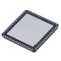
AD9548BCPZ Analog Devices Inc, AD9548BCPZ Datasheet - Page 24

AD9548BCPZ
Manufacturer Part Number
AD9548BCPZ
Description
IC CLOCK GEN/SYNCHRONIZR 88LFCSP
Manufacturer
Analog Devices Inc
Datasheet
1.AD9548BCPZ-REEL7.pdf
(112 pages)
Specifications of AD9548BCPZ
Input
*
Output
*
Frequency - Max
*
Voltage - Supply
*
Operating Temperature
*
Mounting Type
Surface Mount
Package / Case
88-LFCSP
Frequency-max
*
Clock Ic Type
Clock Synthesizer
Ic Interface Type
Serial
Frequency
1GHz
No. Of Outputs
4
No. Of Multipliers / Dividers
4
Supply Current
190mA
Lead Free Status / RoHS Status
Lead free / RoHS Compliant
Available stocks
Company
Part Number
Manufacturer
Quantity
Price
Part Number:
AD9548BCPZ
Manufacturer:
ADI/亚德诺
Quantity:
20 000
Company:
Part Number:
AD9548BCPZ-SMD7
Manufacturer:
SHARP
Quantity:
392
AD9548
GETTING STARTED
POWER-ON RESET
The AD9548 monitors the voltage on the power supplies at
power-up. When DVDD3 is greater than 2.35 V ± 0.1 V and
DVDD (Pin 1, Pin 6, Pin 12, Pin 77, Pin 83, and Pin 88) is
greater than 1.4 V ± 0.05 V, the device generates a 75 ns reset
pulse. The power-up reset pulse is internal and independent of
the RESET pin. This internal power-up reset sequence eliminates
the need for the user to provide external power supply sequencing.
Within 45 ns after the leading edge of the internal reset pulse,
the M0 to M7 multifunction pins behave as high impedance
digital inputs and remain so until programmed otherwise.
INITIAL PIN PROGRAMMING
During a device reset (either via the power-up reset pulse or the
RESET pin), the multifunction pins (M0 to M7) behave as high
impedance inputs, but upon removal of the reset condition,
level-sensitive latches capture the logic pattern present on the
multifunction pins. The AD9548 requires that the user supply
the desired logic state to the M0 to M7 pins by means of pull-up
and/or pull-down resistors (nominally 10 kΩ to 30 kΩ).
The initial state of the M0 to M7 pins following a reset is
referred to as FncInit, Bits[7:0]. Bits[7:0] of FncInit map directly
to the logic states of M7:0, respectively. The three LSBs of
FncInit (FncInit, Bits[2:0]) determine whether the serial port
interface behaves according to the SPI or I
Specifically, FncInit, Bits[2:0] = 000 selects the SPI interface,
while any other value selects the I
the I
The five MSBs of FncInit (FncInit, Bits[7:3]) determine the
operation of the EEPROM loader. On the falling edge of RESET,
if FncInit, Bits[7:3] = 00000, then the EEPROM contents are not
transferred to the control registers and the device registers
assume their default values. However, if FncInit, Bits[7:3] ≠
00000, then the EEPROM controller transfers the contents of
the EEPROM to the control registers with condition = FncInit,
Bits[7:3] (see the EEPROM section).
DEVICE REGISTER PROGRAMMING
The initial state of the M0 to M7 pins establishes the serial I/O
port protocol (SPI or I
protocol, and assuming that an EEPROM download is not used,
program the device according to the recommended sequence
described in the Program the System Clock Functionality
section through the Generate the Output Clock section.
Program the System Clock Functionality
The system clock parameters reside in the 0100 register address
space. They include the following:
2
System clock PLL controls
System clock period
System clock stability timer
C bus address set to the value of FncInit, Bits[2:0].
2
C). Using the appropriate serial port
2
C port with the three LSBs of
2
C protocol.
Rev. A | Page 24 of 112
It is essential to program the system clock period because many of
the AD9548 subsystems rely on this value. It is highly recommended
to program the system clock stability timer, as well. This is
especially important when using the system clock PLL but also
applies if using an external system clock source, especially if the
external source is not expected to be completely stable when
power is applied to the AD9548.
Initialize the System Clock
After the system clock functionality is programmed, issue an
I/O update using Register 0005, Bit 0 to invoke the system clock
settings.
Calibrate the System Clock (Only if Using SYSCLK PLL)
Set the calibrate system clock bit in the sync/cal register
(Address 0A02, Bit 0) and issue an I/O update. Then clear the
calibrate system clock bit and issue another I/O update. This
action allows time for the calibration to proceed while pro-
gramming the remaining device registers.
Program the Multifunction Pins (Optional)
This step is required only if the user intends to use any of the
multifunction pins for status or control. The multifunction pin
parameters reside in the 0200 to 0207 register address space.
The default configuration of the multifunction pins is as an
undesignated high impedance input pin.
Program the IRQ Functionality (Optional)
This step is required only if the user intends to use the IRQ feature.
IRQ control resides in the 0200 to 0207 register address space. It
includes the following:
The IRQ mask default values prevent interrupts from being
generated. The IRQ pin mode default is open-drain NMOS.
Program the Watchdog Timer (Optional)
This step is required only if the user intends to use it. Watchdog
timer control resides in the 0200 register address space. The
watchdog timer is disabled by default.
Program the DAC Full-Scale Current (Optional)
This step is required only if the user intends to use a full-scale
current setting other than the default value. DAC full-scale
current control resides in the 0200 register address space.
Program the Digital Phase-Locked Loop (DPLL)
The DPLL parameters reside in the 0300 register address space.
They include the following:
IRQ pin mode control
IRQ mask
Free-run frequency (DDS frequency tuning word)
DDS phase offset
DPLL pull-in range limits
DPLL closed-loop phase offset
Phase slew control (for hitless reference switching)
Tuning word history control (for holdover operation)


