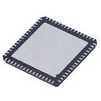
AD9548BCPZ Analog Devices Inc, AD9548BCPZ Datasheet - Page 26

AD9548BCPZ
Manufacturer Part Number
AD9548BCPZ
Description
IC CLOCK GEN/SYNCHRONIZR 88LFCSP
Manufacturer
Analog Devices Inc
Datasheet
1.AD9548BCPZ-REEL7.pdf
(112 pages)
Specifications of AD9548BCPZ
Input
*
Output
*
Frequency - Max
*
Voltage - Supply
*
Operating Temperature
*
Mounting Type
Surface Mount
Package / Case
88-LFCSP
Frequency-max
*
Clock Ic Type
Clock Synthesizer
Ic Interface Type
Serial
Frequency
1GHz
No. Of Outputs
4
No. Of Multipliers / Dividers
4
Supply Current
190mA
Lead Free Status / RoHS Status
Lead free / RoHS Compliant
Available stocks
Company
Part Number
Manufacturer
Quantity
Price
Part Number:
AD9548BCPZ
Manufacturer:
ADI/亚德诺
Quantity:
20 000
Company:
Part Number:
AD9548BCPZ-SMD7
Manufacturer:
SHARP
Quantity:
392
AD9548
THEORY OF OPERATION
OVERVIEW
The AD9548 provides clocking outputs directly related in phase
and frequency to the selected (active) reference but with jitter
characteristics primarily governed by the system clock. The
AD9548 supports up to eight reference inputs and a wide range
of reference frequencies. The core of this product is a digital
phase-locked loop (DPLL). The DPLL has a programmable
digital loop filter that greatly reduces jitter transferred from the
active reference to the output. The AD9548 supports both
manual and automatic holdover. While in holdover, the
AD9548 continues to provide an output as long as the DAC
sample clock is present. The holdover output frequency is a
time average of the output frequency history just prior to the
transition to the holdover condition.
The device offers manual and automatic reference switchover
capability if the active reference is degraded or fails completely.
A direct digital synthesizer (DDS) and integrated DAC consti-
tute a digitally controlled oscillator (DCO). The DCO output is
a sinusoidal signal (450 MHz maximum) at a frequency deter-
mined by the active reference frequency and the programmed
values of the reference prescaler (R) and feedback divider (S).
Although not explicitly shown in Figure 33, the S-divider has
both an integer and fractional component, which is similar to a
fractional-N synthesizer.
M0 TO M7
REFAA
REFBB
REFCC
REFDD
REFA
REFB
REFC
REFD
IRQ
AD9548
4 OR 8
SINGLE-ENDED
DIFFERENTIAL
MONITOR
IRQ AND
STATUS
INPUT
LOGIC
REF
OR
DIGITAL PLL CORE
÷R
CONTROLLER
PHASE
TDC/PFD
Figure 33. Detailed Block Diagram
INTERFACE
CONTROL
DIGITAL
LOGIC
Rev. A | Page 26 of 112
DIGITAL
FILTER
PROG.
LOOP
÷S
HOLDOVER
TW CLAMP
HISTORY
LOGIC
AND
The SYSCLKx input provides the sample clock for the DAC,
which is either a directly applied high frequency source or a low
frequency source coupled with the integrated PLL-based
frequency multiplier. The low frequency option also allows for
the use of a crystal resonator connected directly across the
SYSCLKx inputs.
The DAC output routes directly off-chip, where an external
filter removes the sampling artifacts before returning the signal
on-chip at the CLKINx inputs. Once on-chip, an integrated
comparator converts the filtered sinusoidal signal to a clock
signal (square wave) with very fast rise and fall times.
The clock distribution section provides four output drivers.
Each driver is programmable either as a single differential
LVPECL/LVDS output or as a dual single-ended CMOS output.
Furthermore, each of the four outputs has a dedicated 30-bit
programmable postdivider. The clock distribution section
operates at up to 725 MHz. This enables use of a band-pass
reconstruction filter (for example, a SAW filter) to extract a
Nyquist image from the DAC output spectrum, thereby
allowing output frequencies that exceed the typical 450 MHz
limit at the DAC output.
SYSCLKN SYSCLKP
DDS/DAC
SYSCLK PORT
MULTIPLIER
LOW NOISE
CLOCK
DISTRIBUTION
AMP
POST
POST
POST
POST
DIV
DIV
DIV
DIV
CLOCK
CLKINP
CLKINN
OUT_RSET
OUT0P
OUT0N
OUT1P
OUT1N
OUT2P
OUT2N
OUT3P
OUT3N
EXTERNAL
ANALOG
FILTER


