AD9548BCPZ Analog Devices Inc, AD9548BCPZ Datasheet - Page 2
AD9548BCPZ
Manufacturer Part Number
AD9548BCPZ
Description
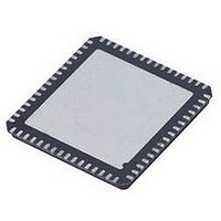
IC CLOCK GEN/SYNCHRONIZR 88LFCSP
Manufacturer
Analog Devices Inc
Datasheet
1.AD9548BCPZ-REEL7.pdf
(112 pages)
Specifications of AD9548BCPZ
Input
*
Output
*
Frequency - Max
*
Voltage - Supply
*
Operating Temperature
*
Mounting Type
Surface Mount
Package / Case
88-LFCSP
Frequency-max
*
Clock Ic Type
Clock Synthesizer
Ic Interface Type
Serial
Frequency
1GHz
No. Of Outputs
4
No. Of Multipliers / Dividers
4
Supply Current
190mA
Lead Free Status / RoHS Status
Lead free / RoHS Compliant
Available stocks
Company
Part Number
Manufacturer
Quantity
Price

Part Number:
AD9548BCPZ
Manufacturer:
ADI/亚德诺
Quantity:
20 000
Company:
Part Number:
AD9548BCPZ-SMD7
Manufacturer:
SHARP
Quantity:
392


AD9548
TABLE OF CONTENTS
Features .............................................................................................. 1
Applications ....................................................................................... 1
General Description ......................................................................... 1
Functional Block Diagram .............................................................. 1
Revision History ............................................................................... 3
Specifications ..................................................................................... 4
Absolute Maximum Ratings .......................................................... 14
Pin Configuration and Function Descriptions ........................... 15
Typical Performance Characteristics ........................................... 18
Input/Output Termination Recommendations .......................... 23
Getting Started ................................................................................ 24
Theory of Operation ...................................................................... 26
Supply Voltage ............................................................................... 4
Supply Current .............................................................................. 4
Power Dissipation ......................................................................... 4
Logic Inputs (M7 to M0, RESET, TDI, TCLK, TMS) .............. 5
Logic Outputs (M7 to M0, IRQ, TDO) ..................................... 5
System Clock Inputs (SYSCLKP/SYSCLKN) ........................... 5
Distribution Clock Inputs (CLKINP/CLKINN) ...................... 6
Reference Inputs (REFA/REFAA to REFD/REFDD) .............. 7
Reference Monitors ...................................................................... 7
Reference Switchover Specifications .......................................... 8
Distribution Clock Outputs (OUT0 to OUT3) ........................ 8
DAC Output Characteristics (DACOUTP/DACOUTN) ....... 9
Time Duration of Digital Functions ........................................ 10
Digital PLL .................................................................................. 10
Digital PLL Lock Detection ...................................................... 10
Holdover Specifications ............................................................. 10
Serial Port Specifications—SPI Mode ...................................... 11
Serial Port Specifications—I
Jitter Generation ......................................................................... 12
ESD Caution ................................................................................ 14
Power-On Reset .......................................................................... 24
Initial Pin Programming ........................................................... 24
Device Register Programming .................................................. 24
Overview ...................................................................................... 26
Reference Clock Inputs .............................................................. 27
Reference Monitors .................................................................... 27
Reference Profiles ....................................................................... 28
Reference Switchover ................................................................. 30
2
C Mode ...................................... 11
Rev. A | Page 2 of 112
Status and Control .......................................................................... 44
Serial Control Port ......................................................................... 51
I/O Programming Registers .......................................................... 58
Register Map ................................................................................... 60
Register Map Bit Descriptions ...................................................... 70
Power Supply Partitions ............................................................... 105
Thermal Performance .................................................................. 106
Digital PLL (DPLL) Core .......................................................... 32
Direct Digital Synthesizer ......................................................... 34
Tuning Word Processing ........................................................... 35
Loop Control State Machine ..................................................... 36
System Clock Inputs ................................................................... 37
SYSCLK PLL Multiplier ............................................................. 38
Clock Distribution ..................................................................... 39
Multifunction Pins (M0 to M7) ............................................... 44
IRQ Pin ........................................................................................ 45
Watchdog Timer ......................................................................... 46
EEPROM ..................................................................................... 46
SPI/I2C Port Selection ................................................................ 51
SPI Serial Port Operation .......................................................... 51
I2C Serial Port Operation .......................................................... 55
Buffered/Active Registers .......................................................... 58
Autoclear Registers ..................................................................... 58
Register Access Restrictions ...................................................... 59
Serial Port Configuration (Register 0000 to Register 0005) . 70
System Clock (Register 0100 to Register 0108) ...................... 71
General Configuration (Register 0200 to Register 0214) ..... 72
DPLL Configuration (Register 0300 to Register 031B)......... 75
Clock Distribution Output Configuration (Register 0400 to
Register 0419) ............................................................................. 77
Reference Input Configuration (Register 0500 to Register
0507) ............................................................................................. 81
Profile Registers (Register 0600 to Register 07FF) ................ 83
Operational Controls (Register 0A00 to Register 0A10) ...... 92
Status Readback (Register 0D00 to Register 0D19) ............... 97
Nonvolatile Memory (EEPROM) Control (Register 0E00 to
Register 0E03) ........................................................................... 100
EEPROM Storage Sequence (Register 0E10 to Register 0E3F)
..................................................................................................... 101
3.3 V Supplies ............................................................................ 105
1.8 V Supplies ............................................................................ 105
Related parts for AD9548BCPZ
Image
Part Number
Description
Manufacturer
Datasheet
Request
R

Part Number:
Description:
Clock Generator Evaluation Board
Manufacturer:
Analog Devices Inc
Datasheet:


Part Number:
Description:
±1.7g Dual-Axis IMEMS Accelerometer Evaluation Board
Manufacturer:
Analog Devices Inc
Datasheet:
Part Number:
Description:
Inertial Sensor Evaluation System
Manufacturer:
Analog Devices Inc
Datasheet:
Part Number:
Description:
Manufacturer:
Analog Devices Inc
Datasheet:
Part Number:
Description:
Manufacturer:
Analog Devices Inc
Datasheet:
Part Number:
Description:
Manufacturer:
Analog Devices Inc
Datasheet:
Part Number:
Description:
Manufacturer:
Analog Devices Inc
Datasheet:
Part Number:
Description:
Manufacturer:
Analog Devices Inc
Datasheet:
Part Number:
Description:
Manufacturer:
Analog Devices Inc
Datasheet:
Part Number:
Description:
Manufacturer:
Analog Devices Inc
Datasheet:
Part Number:
Description:
Manufacturer:
Analog Devices Inc
Datasheet:
Part Number:
Description:
Manufacturer:
Analog Devices Inc
Datasheet: