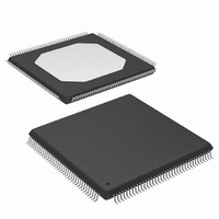
XC3S100E-4TQG144I Xilinx Inc, XC3S100E-4TQG144I Datasheet - Page 104

XC3S100E-4TQG144I
Manufacturer Part Number
XC3S100E-4TQG144I
Description
IC FPGA SPARTAN-3E 100K 144-TQFP
Manufacturer
Xilinx Inc
Series
Spartan™-3Er
Datasheet
1.XC3S100E-4TQG144I.pdf
(193 pages)
Specifications of XC3S100E-4TQG144I
Package / Case
144-TQFP, 144-VQFP
Mounting Type
Surface Mount
Voltage - Supply
1.1 V ~ 3.465 V
Operating Temperature
-40°C ~ 100°C
Number Of I /o
108
Number Of Logic Elements/cells
*
Number Of Gates
*
Lead Free Status / RoHS Status
Lead free / RoHS Compliant
Available stocks
Company
Part Number
Manufacturer
Quantity
Price
Company:
Part Number:
XC3S100E-4TQG144I
Manufacturer:
XILINX/21
Quantity:
163
Company:
Part Number:
XC3S100E-4TQG144I
Manufacturer:
Xilinx Inc
Quantity:
10 000
Part Number:
XC3S100E-4TQG144I
Manufacturer:
XILINX/赛灵思
Quantity:
20 000
DS312-3 (v1.0) March 1, 2005
DC Electrical Characteristics
In this section, specifications may be designated as
Advance, Preliminary, or Production. These terms are
defined as follows:
Advance: Initial estimates are based on simulation, early
characterization, and/or extrapolation from the characteris-
tics of other families. Values are subject to change. Use as
estimates, not for production.
Preliminary: Based on characterization. Further changes
are not expected.
Production: These specifications are approved once the
silicon has been characterized over numerous production
lots. Parameter values are considered stable with no future
changes expected.
Table 1: Absolute Maximum Ratings
DS312-3 (v1.0) March 1, 2005
Advance Product Specification
Notes:
1.
2.
3.
4.
5.
Symbol
V
V
V
V
V
V
T
CCAUX
CCINT
CCO
IN
T
STG
REF
ESD
Stresses beyond those listed under Absolute Maximum Ratings may cause permanent damage to the device. These are stress ratings only;
functional operation of the device at these or any other conditions beyond those listed under the Recommended Operating Conditions is not
implied. Exposure to Absolute Maximum Ratings conditions for extended periods of time adversely affects device reliability.
As a rule, the V
handle overshoot/undershoot as well as achieve PCI compliance. Refer to the following application notes: "Virtex™-II Pro and Spartan-3
3.3V PCI Reference Design" (XAPP653) and "Using 3.3V I/O Guidelines in a Virtex-II Pro Design" (XAPP659).
Each of the User I/O and Dual-Purpose pins is associated with one of the four banks’ V
internal diode junctions that exist between these pins and their associated V
to determine the max limit. When V
that avoids oxide stress is V
All Dedicated pins (PROG_B, DONE, TCK, TDI, TDO, and TMS) draw power from the V
that the internal diode junctions that exist between each of these pins and the V
used to determine the max limit. When V
V
For soldering guidelines, see "Device Packaging and Thermal Characteristics" at www.xilinx.com/bvdocs/userguides/ug112.pdf. Also see
"Implementation and Solder Reflow Guidelines for Pb-Free Packages" at www.xilinx.com/bvdocs/appnotes/xapp427.pdf.
J
IN
(2)
max specification is met, oxide stress is not possible.
Internal supply voltage
Auxiliary supply voltage
Output driver supply voltage
Input reference voltage
Voltage applied to all User I/O pins and
Dual-Purpose pins
Voltage applied to all Dedicated pins
Electrostatic Discharge Voltage
Junction temperature
Storage temperature
© 2005 Xilinx, Inc. All rights reserved. XILINX, the Xilinx logo, and other designated brands included herein are trademarks of Xilinx, Inc.
IN
limits apply to both the DC and AC components of signals. Simple application solutions are available that show how to
Description
INX
R
= 4.05V. As long as the V
CCO
is at its maximum recommended operating level (3.45V), V
CCAUX
All other trademarks are the property of their respective owners.
is at its maximum recommended operating level (2.625V), V
IN
018
0
Driver in a high-impedance state
Human body model
Charged device model
Machine model
www.xilinx.com
max specification is met, oxide stress is not possible.
0
Spartan-3E FPGA Family:
DC and Switching
Characteristics
Advance Product Specification
All parameter limits are representative of worst-case supply
voltage and junction temperature conditions. The following
applies unless otherwise noted: The parameter values
published in this module apply to all Spartan™-3E
devices. AC and DC characteristics are specified using
the same numbers for both commercial and industrial
grades.
If a particular Spartan-3E FPGA differs in functional
behavior or electrical characteristic from this data
sheet, those differences are described in a separate
errata document. The errata documents for Spartan-3E
FPGAs are living documents and are available
Conditions
CCO
CCAUX
rails do not turn on.
rail do not turn on.
CCO
CCAUX
rails. Meeting the V
rail (2.5V). Meeting the V
IN
Table 4
–2000
–500
–200
–0.5
–0.5
–0.5
–0.5
–0.5
–0.5
Min
–65
max is 3.95V. The maximum voltage
-
Table 4
IN
specifies the V
max < 3.125V. As long as the
IN
specifies the V
V
V
max limit ensures that the
V
CCAUX
CCO
CCO
+2000
+500
+200
Max
3.00
1.32
3.75
125
150
IN
+ 0.5
+ 0.5
+ 0.5
max limit ensures
CCO
(3)
(3)
(4)
CCAUX
range used
online
Units
range
°C
°C
V
V
V
V
V
V
V
V
V
.
1


