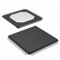
XC3S100E-4TQG144I Xilinx Inc, XC3S100E-4TQG144I Datasheet - Page 38

XC3S100E-4TQG144I
Manufacturer Part Number
XC3S100E-4TQG144I
Description
IC FPGA SPARTAN-3E 100K 144-TQFP
Manufacturer
Xilinx Inc
Series
Spartan™-3Er
Datasheet
1.XC3S100E-4TQG144I.pdf
(193 pages)
Specifications of XC3S100E-4TQG144I
Package / Case
144-TQFP, 144-VQFP
Mounting Type
Surface Mount
Voltage - Supply
1.1 V ~ 3.465 V
Operating Temperature
-40°C ~ 100°C
Number Of I /o
108
Number Of Logic Elements/cells
*
Number Of Gates
*
Lead Free Status / RoHS Status
Lead free / RoHS Compliant
Available stocks
Company
Part Number
Manufacturer
Quantity
Price
Company:
Part Number:
XC3S100E-4TQG144I
Manufacturer:
XILINX/21
Quantity:
163
Company:
Part Number:
XC3S100E-4TQG144I
Manufacturer:
Xilinx Inc
Quantity:
10 000
Part Number:
XC3S100E-4TQG144I
Manufacturer:
XILINX/赛灵思
Quantity:
20 000
Table 20: Block RAM Port Signals (Continued)
Block RAM Attribute Definitions
A block RAM has a number of attributes that control its
behavior as shown in
Table 21: Block RAM Attributes
DS312-2 (v1.1) March 21, 2005
Advance Product Specification
Data Output Bus
Parity Data
Output(s)
Write Enable
Clock Enable
Set/Reset
Clock
Initial Content for Data Memory, Loaded
during Configuration
Initial Content for Parity Memory, Loaded
during Configuration
Data Output Latch Initialization
Description
Signal
R
Function
Table
Port A
Signal
Name
DOPA
SSRA
CLKA
WEA
DOA
ENA
21.
Signal
Port B
DOPB
Name
SSRB
CLKB
DOB
WEB
ENB
Direction
INITxx (INIT_00 through
INITA, INITB (dual-port)
Output
Output
Input
Input
Input
Input
INITPxx (INITP_00
INIT (single-port)
through INITP0F)
Attribute
www.xilinx.com
INIT3F)
Data is written to the DO output bus from the RAM location
specified by the address input bus, ADDR. See the DI signal
description for DO port width configurations.
Basic data access occurs on the active edge of the CLK when
WE is inactive and EN is active. The DO outputs mirror the data
stored in the address ADDR memory location. Data access with
WE active if the WRITE_MODE attribute is set to the value:
WRITE_FIRST, which accesses data after the write takes place.
READ_FIRST accesses data before the write occurs. A third
attribute, NO_CHANGE, latches the DO outputs upon the
assertion of WE. See
the WRITE_MODE attribute.
Parity outputs represent additional bits included in the data input
path. The number of parity bits ‘p’ included in the DI bus (same
as for the DO bus) depends on a port’s total data path width (w).
See the DIP signal description for configuration details.
When asserted together with EN, this input enables the writing of
data to the RAM. When WE is inactive with EN asserted, read
operations are still possible. In this case, a latch passes data
from the addressed memory location to the DO outputs.
When asserted, this input enables the CLK signal to perform
read and write operations to the block RAM. When inactive, the
block RAM does not perform any read or write operations.
When asserted, this pin forces the DO output latch to the value
of the SRVAL attribute. It is synchronized to the CLK signal.
This input accepts the clock signal to which read and write
operations are synchronized. All associated port inputs are
required to meet setup times with respect to the clock signal’s
active edge. The data output bus responds after a clock-to-out
delay referenced to the clock signal’s active edge.
Each initialization string defines 32 hex values
of the 16384-bit data memory of the block RAM.
Each initialization string defines 32 hex values
of the 2048-bit parity data memory of the block
RAM.
Hex value the width of the chosen port.
Block RAM Data Operations
Function
Possible Values
Functional Description
for details on
31


