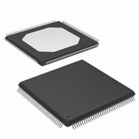
XC3S100E-4TQG144I Xilinx Inc, XC3S100E-4TQG144I Datasheet - Page 59

XC3S100E-4TQG144I
Manufacturer Part Number
XC3S100E-4TQG144I
Description
IC FPGA SPARTAN-3E 100K 144-TQFP
Manufacturer
Xilinx Inc
Series
Spartan™-3Er
Datasheet
1.XC3S100E-4TQG144I.pdf
(193 pages)
Specifications of XC3S100E-4TQG144I
Package / Case
144-TQFP, 144-VQFP
Mounting Type
Surface Mount
Voltage - Supply
1.1 V ~ 3.465 V
Operating Temperature
-40°C ~ 100°C
Number Of I /o
108
Number Of Logic Elements/cells
*
Number Of Gates
*
Lead Free Status / RoHS Status
Lead free / RoHS Compliant
Available stocks
Company
Part Number
Manufacturer
Quantity
Price
Company:
Part Number:
XC3S100E-4TQG144I
Manufacturer:
XILINX/21
Quantity:
163
Company:
Part Number:
XC3S100E-4TQG144I
Manufacturer:
Xilinx Inc
Quantity:
10 000
Part Number:
XC3S100E-4TQG144I
Manufacturer:
XILINX/赛灵思
Quantity:
20 000
- Current page: 59 of 193
- Download datasheet (2Mb)
Functional Description
The outputs of the top or bottom BUFGMUX elements con-
nect to two vertical spines, each comprising four vertical
clock lines as shown in
these clock signals connect to the eight-line horizontal clock
spine.
Outputs of the left and right BUFGMUX elements are routed
onto the left or right horizontal spines, each comprising
eight horizontal clock lines.
Each of the eight clock signals in a clock quadrant derives
either from a global clock signal or a half clock signal. In
other words, there are up to 24 total potential clock inputs to
the FPGA, eight of which can connect to clocked elements
52
Figure 44: Clock Sources for the Eight Clock Lines within a Clock Quadrant
a. Left (TL and BL Quadrants) Half of Die
BUFGMUX Output
X0Y2 (Left Half)
X0Y3 (Left Half)
X0Y4 (Left Half)
X0Y5 (Left Half)
X0Y6 (Left Half)
X0Y7 (Left Half)
X0Y8 (Left Half)
X0Y9 (Left Half)
X2Y11 (Global)
X2Y10 (Global)
X1Y11 (Global)
X1Y10 (Global)
X2Y1 (Global)
X2Y0 (Global)
X1Y1 (Global)
X1Y0 (Global)
Figure
42. At the center of the die,
Clock Line
www.xilinx.com
A
B
C
D
E
F
G
H
b. Right (TR and BR Quadrants) Half of Die
X3Y2 (Right Half)
X3Y3 (Right Half)
X3Y4 (Right Half)
X3Y5 (Right Half)
X3Y6 (Right Half)
X3Y7 (Right Half)
X3Y8 (Right Half)
X3Y9 (Right Half)
in a single clock quadrant.
lines in each quadrant are selected from associated BUFG-
MUX sources. For example, if quadrant clock ‘A’ in the bot-
tom left (BL) quadrant originates from BUFGMUX_X2Y1,
then the clock signal from BUFGMUX_X0Y2 is unavailable
in the bottom left quadrant. However, the top left (TL) quad-
rant clock ‘A’ can still solely use the output from either
BUFGMUX_X2Y1 or BUFGMUX_X0Y2 as the source.
To minimize the dynamic power dissipation of the clock net-
work, the Xilinx development software automatically dis-
ables all clock segments not in use.
BUFGMUX Output
X2Y11 (Global)
X2Y10 (Global)
X1Y11 (Global)
X1Y10 (Global)
X2Y1 (Global)
X2Y0 (Global)
X1Y1 (Global)
X1Y0 (Global)
DS312-2_17_030105
Figure 44
Advance Product Specification
Clock Line
DS312-2 (v1.1) March 21, 2005
A
B
C
D
E
F
G
H
shows how the clock
R
Related parts for XC3S100E-4TQG144I
Image
Part Number
Description
Manufacturer
Datasheet
Request
R

Part Number:
Description:
IC SPARTAN-3E FPGA 100K 144-TQFP
Manufacturer:
Xilinx Inc
Datasheet:

Part Number:
Description:
FIELD PROGRAMMER
Manufacturer:
Xilinx Inc
Datasheet:

Part Number:
Description:
FPGA Spartan®-3E Family 100K Gates 2160 Cells 572MHz 90nm (CMOS) Technology 1.2V 100-Pin VTQFP
Manufacturer:
Xilinx Inc
Datasheet:

Part Number:
Description:
FPGA Spartan®-3E Family 100K Gates 2160 Cells 572MHz 90nm (CMOS) Technology 1.2V 144-Pin TQFP
Manufacturer:
Xilinx Inc
Datasheet:

Part Number:
Description:
FPGA Spartan®-3E Family 100K Gates 2160 Cells 657MHz 90nm (CMOS) Technology 1.2V 144-Pin TQFP
Manufacturer:
Xilinx Inc
Datasheet:

Part Number:
Description:
Spartan-3E FPGA Family
Manufacturer:
XILINX [Xilinx, Inc]
Datasheet:

Part Number:
Description:
Spartan-3E FPGA Family: Complete Data Sheet
Manufacturer:
XILINX [Xilinx, Inc]
Datasheet:

Part Number:
Description:
IC FPGA SPARTAN-3E 100K 100-VQFP
Manufacturer:
Xilinx Inc
Datasheet:

Part Number:
Description:
IC FPGA SPARTAN-3E 100K 132CSBGA
Manufacturer:
Xilinx Inc
Datasheet:

Part Number:
Description:
IC FPGA SPARTAN-3E 100K 132CSBGA
Manufacturer:
Xilinx Inc
Datasheet:

Part Number:
Description:
IC FPGA SPARTAN-3E 100K 144-TQFP
Manufacturer:
Xilinx Inc
Datasheet:

Part Number:
Description:
IC FPGA SPARTAN 3E 100VQFP
Manufacturer:
Xilinx Inc
Datasheet:

Part Number:
Description:
IC FPGA SPARTAN 3E 144TQFP
Manufacturer:
Xilinx Inc
Datasheet:

Part Number:
Description:
FPGA Spartan®-3E Family 100K Gates 2160 Cells 572MHz 90nm (CMOS) Technology 1.2V 132-Pin CSBGA
Manufacturer:
Xilinx Inc
Datasheet:

Part Number:
Description:
IC CPLD .8K 36MCELL 44-VQFP
Manufacturer:
Xilinx Inc
Datasheet:


