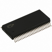
CY7C66113-PVC Cypress Semiconductor Corp, CY7C66113-PVC Datasheet - Page 20

CY7C66113-PVC
Manufacturer Part Number
CY7C66113-PVC
Description
IC MCU 8K USB HUB 4 PORT 56TSSOP
Manufacturer
Cypress Semiconductor Corp
Specifications of CY7C66113-PVC
Applications
USB Hub/Microcontroller
Core Processor
M8
Program Memory Type
OTP (8 kB)
Controller Series
USB Hub
Ram Size
256 x 8
Interface
I²C, USB, HAPI
Number Of I /o
31
Voltage - Supply
4 V ~ 5.5 V
Operating Temperature
0°C ~ 70°C
Mounting Type
Surface Mount
Package / Case
56-SSOP
Operating Temperature (max)
70C
Operating Temperature (min)
0C
Operating Temperature Classification
Commercial
Mounting
Surface Mount
Pin Count
56
Lead Free Status / RoHS Status
Contains lead / RoHS non-compliant
For Use With
CY3649 - PROGRAMMER HI-LO USB M8428-1339 - KIT LOW SPEED PERSONALITY BOARD
Lead Free Status / RoHS Status
Not Compliant, Contains lead / RoHS non-compliant
Other names
428-1330
Available stocks
Company
Part Number
Manufacturer
Quantity
Price
Company:
Part Number:
CY7C66113-PVC
Manufacturer:
CY
Quantity:
10
There are up to 31 GPIO pins (P0[7:0], P1[7:0], P2[7:0], and P3[6:0]) for the hardware interface. The number of GPIO pins
changes based on the package type of the chip. Each port can be configured as inputs with internal pull-ups, open drain outputs,
or traditional CMOS outputs. Port 3 offers a higher current drive, with typical current sink capability of 12 mA. The data for each
GPIO port is accessible through the data registers. Port data registers are shown in Figure 9-2 through Figure 9-5, and are set
to 1 on reset.
Port 0 Data
Port 1 Data
Port 3 Data
Special care should be taken with any unused GPIO data bits. An unused GPIO data bit, either a pin on the chip or a port bit that
is not bonded on a particular package, must not be left floating when the device enters the suspend state. If a GPIO data bit is
left floating, the leakage current caused by the floating bit may violate the suspend current limitation specified by the USB
specifications. If a ‘1’ is written to the unused data bit and the port is configured with open drain outputs, the unused data bit
remains in an indeterminate state. Therefore, if an unused port bit is programmed in open-drain mode, it must be written with a
‘0.’ Notice that the CY7C66013 always requires that P3[7:5] be written with a ‘0.’ When the CY7C66113 is used the P3[7] should
be written with a ‘0.’
In normal non-HAPI mode, reads from a GPIO port always return the present state of the voltage at the pin, independent of the
settings in the Port Data Registers. If HAPI mode is activated for a port, reads of that port return latched data as controlled by the
HAPI signals (see Section 14.0). During reset, all of the GPIO pins are set to a high impedance input state (‘1’ in open drain
mode). Writing a ‘0’ to a GPIO pin drives the pin LOW. In this state, a ‘0’ is always read on that GPIO pin unless an external source
overdrives the internal pull-down device.
9.1
Every GPIO port can be programmed as inputs with internal pull-ups, outputs LOW or HIGH, or Hi-Z (floating, the pin is not driven
internally). In addition, the interrupt polarity for each port can be programmed. The Port Configuration bits (Figure 9-6) and the
Interrupt Enable bit (Figure 9-7 through Figure 9-10) determine the interrupt polarity of the port pins.
GPIO Configuration
Document #: 38-08024 Rev. *A
Bit #
Bit Name
Read/Write
Reset
Bit #
Bit Name
Read/Write
Reset
Bit #
Bit Name
Read/Write
Reset
Bit #
Bit Name
Read/Write
Reset
Bit #
Bit Name
Read/Write
Reset
Port 2 Data
GPIO Configuration Port
7
P0.7
R/W
1
7
P1.7
R/W
1
7
P2.7
R/W
1
7
Reserved
R/W
1
7
Port 3
Config Bit 1
R/W
0
6
P0.6
R/W
1
6
P1.6
R/W
1
6
P2.6
R/W
1
6
Reserved
R/W
1
6
Port 3
Config Bit 0
R/W
0
Figure 9-6. GPIO Configuration Register
5
P0.5
R/W
1
5
P1.5
R/W
1
5
P2.5
R/W
1
5
Reserved
R/W
1
5
Port 2
Config Bit 1
R/W
0
Figure 9-2. Port 0 Data
Figure 9-4. Port 2 Data
Figure 9-5. Port 3 Data
Figure 9-3. Port1 Data
4
P0.4
R/W
1
4
P1.4
R/W
1
4
P2.4
R/W
1
4
Reserved
R/W
1
4
Port 2
Config Bit 0
R/W
0
3
P0.3
R/W
1
3
Reserved
R/W
1
3
P2.3
R/W
1
3
Reserved
R/W
1
3
Port 1
Config Bit 1
R/W
0
2
P0.2
R/W
1
2
P1.2
R/W
1
2
Reserved
R/W
1
2
Reserved
R/W
1
2
Port 1
Config Bit 0
R/W
0
1
P0.1
R/W
1
1
P1.1
R/W
1
1
Reserved
R/W
1
1
P3.1
R/W
1
1
Port 0
Config Bit 1
R/W
0
CY7C66013
CY7C66113
Page 20 of 58
ADDRESS 0x03
ADDRESS 0x00
0
P0.0
R/W
1
ADDRESS 0x01
0
P1.0
R/W
1
ADDRESS 0x02
0
Reserved
R/W
1
0
P3.0
R/W
1
0
Port 0
Config Bit 0
R/W
0
ADDRESS 0x08


