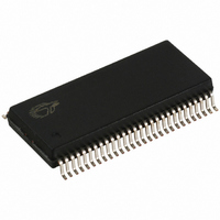
CY7C66113-PVC Cypress Semiconductor Corp, CY7C66113-PVC Datasheet - Page 31

CY7C66113-PVC
Manufacturer Part Number
CY7C66113-PVC
Description
IC MCU 8K USB HUB 4 PORT 56TSSOP
Manufacturer
Cypress Semiconductor Corp
Specifications of CY7C66113-PVC
Applications
USB Hub/Microcontroller
Core Processor
M8
Program Memory Type
OTP (8 kB)
Controller Series
USB Hub
Ram Size
256 x 8
Interface
I²C, USB, HAPI
Number Of I /o
31
Voltage - Supply
4 V ~ 5.5 V
Operating Temperature
0°C ~ 70°C
Mounting Type
Surface Mount
Package / Case
56-SSOP
Operating Temperature (max)
70C
Operating Temperature (min)
0C
Operating Temperature Classification
Commercial
Mounting
Surface Mount
Pin Count
56
Lead Free Status / RoHS Status
Contains lead / RoHS non-compliant
For Use With
CY3649 - PROGRAMMER HI-LO USB M8428-1339 - KIT LOW SPEED PERSONALITY BOARD
Lead Free Status / RoHS Status
Not Compliant, Contains lead / RoHS non-compliant
Other names
428-1330
Available stocks
Company
Part Number
Manufacturer
Quantity
Price
Company:
Part Number:
CY7C66113-PVC
Manufacturer:
CY
Quantity:
10
Although Reset is not an interrupt, the first instruction executed after a reset is at PROM address 0x0000h—which corresponds
to the first entry in the Interrupt Vector Table. Because the JMP instruction is two bytes long, the interrupt vectors occupy two bytes.
Table 16-1. Interrupt Vector Assignments
16.2
Interrupt latency can be calculated from the following equation:
Interrupt latency =
For example, if a five-clock cycle instruction such as JC is being executed when an interrupt occurs, the first instruction of the
Interrupt Service Routine executes a minimum of 16 clocks (1+10+5) or a maximum of 20 clocks (5+10+5) after the interrupt is
issued. For a 12-MHz internal clock (6-MHz crystal), 20 clock periods is 20/12 MHz = 1.667 s.
16.3
The USB Controller recognizes a USB Reset when a Single Ended Zero (SE0) condition persists on the upstream USB port for
12–16 s. SE0 is defined as the condition in which both the D+ line and the D– line are LOW. A USB Bus Reset may be recognized
for an SE0 as short as 12 s, but is always recognized for an SE0 longer than 16 s. When a USB Bus Reset is detected, bit 5
of the Processor Status and Control Register (Figure 15-1) is set to record this event. In addition, the controller clears the following
registers:
A USB Bus Reset Interrupt is generated at the end of the USB Bus Reset condition when the SE0 state is deasserted. If the USB
reset occurs during the start-up delay following a POR, the delay is aborted as described in Section 7.1.
16.4
There are two periodic timer interrupts: the 128- s interrupt and the 1.024-ms interrupt. The user should disable both timer
interrupts before going into the suspend mode to avoid possible conflicts between servicing the timer interrupts first or the suspend
request first.
Document #: 38-08024 Rev. *A
Not Applicable
1
2
3
4
5
6
7
8
9
10
11
12
SIE Section:
Hub Section:
Interrupt Vector Number
Interrupt Latency
USB Bus Reset Interrupt
Timer Interrupt
Hub Ports Enable (0x49)
Hub Ports Speed (0x4A)
Hub Ports Suspend (0x4D)
Hub Ports Resume Status (0x4E)
Hub Ports SE0 Status (0x4F)
Hub Ports Data (0x50)
Hub Downstream Force (0x51).
USB Device Address Registers (0x10, 0x40)
Hub Ports Connect Status (0x48)
(Number of clock cycles remaining in the current instruction) + (10 clock cycles for the CALL instruction) +
(5 clock cycles for the JMP instruction).
0x0000
0x0002
0x0004
0x0006
0x0008
0x000A
0x000C
0x000E
0x0010
0x0012
0x0014
0x0016
0x0018
ROM Address
Execution after Reset begins here
USB Bus Reset interrupt
128- s timer interrupt
1.024-ms timer interrupt
USB Address A Endpoint 0 interrupt
USB Address A Endpoint 1 interrupt
USB Address A Endpoint 2 interrupt
USB Address B Endpoint 0 interrupt
USB Address B Endpoint 1 interrupt
USB Hub interrupt
DAC interrupt
GPIO interrupt
I
2
C interrupt
Function
CY7C66013
CY7C66113
Page 31 of 58


