CY7C66113-PVC Cypress Semiconductor Corp, CY7C66113-PVC Datasheet - Page 25
CY7C66113-PVC
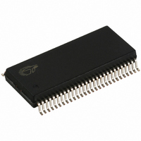
Manufacturer Part Number
CY7C66113-PVC
Description
IC MCU 8K USB HUB 4 PORT 56TSSOP
Manufacturer
Cypress Semiconductor Corp
Specifications of CY7C66113-PVC
Applications
USB Hub/Microcontroller
Core Processor
M8
Program Memory Type
OTP (8 kB)
Controller Series
USB Hub
Ram Size
256 x 8
Interface
I²C, USB, HAPI
Number Of I /o
31
Voltage - Supply
4 V ~ 5.5 V
Operating Temperature
0°C ~ 70°C
Mounting Type
Surface Mount
Package / Case
56-SSOP
Operating Temperature (max)
70C
Operating Temperature (min)
0C
Operating Temperature Classification
Commercial
Mounting
Surface Mount
Pin Count
56
Lead Free Status / RoHS Status
Contains lead / RoHS non-compliant
For Use With
CY3649 - PROGRAMMER HI-LO USB M8428-1339 - KIT LOW SPEED PERSONALITY BOARD
Lead Free Status / RoHS Status
Not Compliant, Contains lead / RoHS non-compliant
Other names
428-1330
Available stocks
Company
Part Number
Manufacturer
Quantity
Price
Company:

Part Number:
CY7C66113-PVC
Manufacturer:
CY
Quantity:
10


Note:
Bits [7,1:0] of the HAPI/I
Bits [5:2] are used in HAPI mode only, and are described in Section 14.0. Table 12-1 shows the HAPI port configurations, and
Table 12-2 shows I
packages, and to allow simultaneous HAPI and I
HAPI operation is enabled whenever either HAPI Port Width Bit (Bit 1 or 0) is non-zero. This affects GPIO operation as described
in Section 14.0. The I
Table 12-1. HAPI Port Configuration
Table 12-2. I
13.0
The I
multi-master modes of operation. The I
interrupts as needed to allow firmware to take appropriate action during transactions. While waiting for firmware response, the
hardware keeps the I
The I
a stop bit is detected by the slave when in receive mode, or when arbitration is lost. Details of the interrupt responses are given
in Section 16.9.
The I
(Figure 13-2). The Data Register is implemented as separate read and write registers. Generally, the I
Register should only be monitored after the I
read misleading bit status if a transaction is underway.
The I
1 or GPIO port 2. Refer to Section 12.0 for the bit definitions and functionality of the HAPI/I
used to set the locations of the configurable I
Status & Control Register, the two LSB ([1:0]) of the corresponding GPIO port is placed in Open Drain mode, regardless of the
settings of the GPIO Configuration Register. The electrical characteristics of the I
GPIO ports 1 and 2. Note that the I
All control of the I
I
Bits [7..0] : I
Document #: 38-08024 Rev. *A
I
2
2
Reset
3.
Bit #
Bit Name
Read/Write
Reset
Bit #
11
10
01
00
Don’t Care
0
1
C Data
C Status and Control
I
2
2
2
2
2
C-compatible function must be separately enabled, as described in Section 13.0.
I
C-compatible interface consists of two registers, an I
Contains 8-bit data on the I
2
C-compatible interface generates an interrupt to the microcontroller at the end of each received or transmitted byte, when
C SCL clock is connected to bit 0 of GPIO port 1 or GPIO port 2, and the I
C-compatible block provides a versatile two-wire communication with external devices, supporting master, slave, and
C Position (Bit 7, Figure 12-1)
I
2
C-compatible Controller
Port Width (Bit 0 and 1, Figure 12-1)
2
2
C Data
C Port Configuration
0
7
R/W
X
7
I
2
C Data 7
2
C clock and data lines is performed by the I
2
C pin location configuration options. These I
2
2
C-compatible bus idle if necessary.
C-compatible interface must be separately enabled as described in Section13.0.
2
C Configuration Register control the pin out configuration of the HAPI and I
0
6
R/W
X
6
I
2
C Data 6
2
C Bus.
OL
(max) is 2 mA @ V
2
C-compatible block functions by handling the low-level signaling in hardware, and issuing
Figure 12-1. HAPI/I
Figure 13-2. I
0
5
R/W
X
5
I
2
2
1
0
0
2
C Data 5
C interrupt, as all bits are valid at that time. Polling this register at other times could
C pins. Once the I
I
Figure 13-1. I
2
2
C Port Width (Bit 1, Figure 12-1)
C-compatible operation.
2
C Status and Control Register
OL
0
4
R/W
X
4
2
I
2
C Data Register (Figure 13-1) and an I
C Data 4
2
= 2.0V for ports 1 and 2.
C Configuration Register
2
2
C Data Register
C-compatible block.
16 Bits: P1[7:0], P0[7:0]
8 Bits: P0[7:0]
24 Bits: P3[7:0], P1[7:0], P0[7:0]
No HAPI Interface
2
C-compatible functionality is enabled by setting bit 0 of the I
2
C-compatible options exist due to pin limitations in certain
0
3
R/W
X
3
I
2
C Data 3
2
C SDA data is connected to bit 1 of GPIO port
2
C-compatible interface is the same as that of
0
2
R/W
X
2
I
HAPI Port Width
2
C Data 2
I
I
I
I
2
2
2
2
C Position
C on P2[1:0], 0:SCL, 1:SDA
C on P1[1:0], 0:SCL, 1:SDA
C on P2[1:0], 0:SCL, 1:SDA
2
C Configuration Register, which is
2
C Status and Control Register
0
1
R/W
X
1
I
2
C Data 1
2
C-compatible interfaces.
2
C Status and Control
CY7C66013
CY7C66113
Page 25 of 58
0
0
R/W
X
0
ADDRESS 0x28
ADDRESS 0x29
I
2
C Data 0
2
C
Related parts for CY7C66113-PVC
Image
Part Number
Description
Manufacturer
Datasheet
Request
R

Part Number:
Description:
Manufacturer:
Cypress Semiconductor Corp
Datasheet:
Part Number:
Description:
Manufacturer:
Cypress Semiconductor Corp
Datasheet:
Part Number:
Description:
Manufacturer:
Cypress Semiconductor Corp
Datasheet:
Part Number:
Description:
Manufacturer:
Cypress Semiconductor Corp
Datasheet:
Part Number:
Description:
Manufacturer:
Cypress Semiconductor Corp
Datasheet: