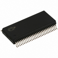
CY7C66113-PVC Cypress Semiconductor Corp, CY7C66113-PVC Datasheet - Page 28

CY7C66113-PVC
Manufacturer Part Number
CY7C66113-PVC
Description
IC MCU 8K USB HUB 4 PORT 56TSSOP
Manufacturer
Cypress Semiconductor Corp
Specifications of CY7C66113-PVC
Applications
USB Hub/Microcontroller
Core Processor
M8
Program Memory Type
OTP (8 kB)
Controller Series
USB Hub
Ram Size
256 x 8
Interface
I²C, USB, HAPI
Number Of I /o
31
Voltage - Supply
4 V ~ 5.5 V
Operating Temperature
0°C ~ 70°C
Mounting Type
Surface Mount
Package / Case
56-SSOP
Operating Temperature (max)
70C
Operating Temperature (min)
0C
Operating Temperature Classification
Commercial
Mounting
Surface Mount
Pin Count
56
Lead Free Status / RoHS Status
Contains lead / RoHS non-compliant
For Use With
CY3649 - PROGRAMMER HI-LO USB M8428-1339 - KIT LOW SPEED PERSONALITY BOARD
Lead Free Status / RoHS Status
Not Compliant, Contains lead / RoHS non-compliant
Other names
428-1330
Available stocks
Company
Part Number
Manufacturer
Quantity
Price
Company:
Part Number:
CY7C66113-PVC
Manufacturer:
CY
Quantity:
10
In this case (see Figure 25-4), the external device drives the STB and CS pins active (LOW) when it drives new data onto the
port pins. When this happens, the internal latches become full, which causes the Latch Empty bit to be deasserted. When STB
is returned HIGH (inactive), the HAPI/GPIO interrupt is generated. Firmware then reads the parallel ports to empty the HAPI
latches. If 16-bit or 24-bit transfers are being made, Port 0 should be read last because reads from Port 0 assert the Latch Empty
bit and the LatEmptyPin to signal the external device for more data.
The Latch Empty bit reads the opposite state from the external LatEmptyPin on pin P2[2]. If the LEMPTY Polarity bit is 0,
LatEmptyPin is active HIGH, and the Latch Empty bit is active LOW.
15.0
Processor Status and Control
Bit 0: Run
Bit 1: Reserved
Bit 2: Interrupt Enable Sense
Bit 3: Suspend
Bit 4: Power-on Reset
Bit 5: USB Bus Reset Interrupt
Bit 6: WDR
Bit 7: IRQ Pending
During power-up, the Processor Status and Control Register is set to 00010001, which indicates a POR (bit 4 set) has occurred
and no interrupts are pending (bit 7 clear). During the 96 ms suspend at start-up (explained in Section 7.1), a WDR also occurs
unless this suspend is aborted by an upstream SE0 before 8 ms. If a WDR occurs during the power-up suspend interval, firmware
reads 01010001 from the Status and Control Register after power-up. Normally, the POR bit should be cleared so a subsequent
WDR can be clearly identified. If an upstream bus reset is received before firmware examines this register, the Bus Reset bit may
also be set.
Document #: 38-08024 Rev. *A
Bit #
Bit Name
Read/Write
Reset
This bit is manipulated by the HALT instruction. When Halt is executed, all the bits of the Processor Status and Control
Register are cleared to 0. Since the run bit is cleared, the processor stops at the end of the current instruction. The processor
remains halted until an appropriate reset occurs (power-on or Watchdog). This bit should normally be written as a ‘1.’
Bit 1 is reserved and must be written as a zero.
This bit indicates whether interrupts are enabled or disabled. Firmware has no direct control over this bit as writing a zero
or one to this bit position has no effect on interrupts. A ‘0’ indicates that interrupts are masked off and a ‘1’ indicates that
the interrupts are enabled. This bit is further gated with the bit settings of the Global Interrupt Enable Register (Figure 16-1)
and USB End Point Interrupt Enable Register (Figure 16-2). Instructions DI, EI, and RETI manipulate the state of this bit.
Writing a ‘1’ to the Suspend bit halts the processor and cause the microcontroller to enter the suspend mode that signifi-
cantly reduces power consumption. A pending, enabled interrupt or USB bus activity causes the device to come out of
suspend. After coming out of suspend, the device resumes firmware execution at the instruction following the IOWR which
put the part into suspend. An IOWR attempting to put the part into suspend is ignored if USB bus activity is present. See
Section 8.0 for more details on suspend mode operation.
The Power-on Reset is set to ‘1’ during a power-on reset. The firmware can check bits 4 and 6 in the reset handler to
determine whether a reset was caused by a power-on condition or a Watchdog timeout. A POR event may be followed by
a WDR before firmware begins executing, as explained below.
The USB Bus Reset Interrupt bit is set when the USB Bus Reset is detected on receiving a USB Bus Reset signal on the
upstream port. The USB Bus Reset signal is a single-ended zero (SE0) that lasts from 12 to 16 s. An SE0 is defined as
the condition in which both the D+ line and the D– line are LOW at the same time.
The WDR is set during a reset initiated by the WDT. This indicates the WDT went for more than t
between Watchdog clears. This can occur with a POR event, as noted below.
The IRQ pending, when set, indicates that one or more of the interrupts has been recognized as active. An interrupt remains
pending until its interrupt enable bit is set (Figure 16-1, Figure 16-2) and interrupts are globally enabled. At that point, the
internal interrupt handling sequence clears this bit until another interrupt is detected as pending.
Processor Status and Control Register
7
IRQ
Pending
R
0
6
Reset
R/W
0
Watchdog
Figure 15-1. Processor Status and Control Register
5
USB Bus Reset
Interrupt
R/W
0
4
Power-On
Reset
R/W
1
3
R/W
0
Suspend
2
Interrupt
Enable Sense
R
0
1
R/W
0
Reserved
WATCH
CY7C66013
CY7C66113
(8 ms minimum)
Page 28 of 58
ADDRESS 0xFF
0
Run
R/W
1


