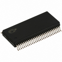
CY7C66113-PVC Cypress Semiconductor Corp, CY7C66113-PVC Datasheet - Page 22

CY7C66113-PVC
Manufacturer Part Number
CY7C66113-PVC
Description
IC MCU 8K USB HUB 4 PORT 56TSSOP
Manufacturer
Cypress Semiconductor Corp
Specifications of CY7C66113-PVC
Applications
USB Hub/Microcontroller
Core Processor
M8
Program Memory Type
OTP (8 kB)
Controller Series
USB Hub
Ram Size
256 x 8
Interface
I²C, USB, HAPI
Number Of I /o
31
Voltage - Supply
4 V ~ 5.5 V
Operating Temperature
0°C ~ 70°C
Mounting Type
Surface Mount
Package / Case
56-SSOP
Operating Temperature (max)
70C
Operating Temperature (min)
0C
Operating Temperature Classification
Commercial
Mounting
Surface Mount
Pin Count
56
Lead Free Status / RoHS Status
Contains lead / RoHS non-compliant
For Use With
CY3649 - PROGRAMMER HI-LO USB M8428-1339 - KIT LOW SPEED PERSONALITY BOARD
Lead Free Status / RoHS Status
Not Compliant, Contains lead / RoHS non-compliant
Other names
428-1330
Available stocks
Company
Part Number
Manufacturer
Quantity
Price
Company:
Part Number:
CY7C66113-PVC
Manufacturer:
CY
Quantity:
10
Port 1 Interrupt Enable
Port 2 Interrupt Enable
Port 3 Interrupt Enable
10.0
The CY7C66113 features a programmable sink current 8 bit port which is also known as DAC port. Each of these port I/O pins
have a programmable current sink. Writing a ‘1’ to a DAC I/O pin disables the output current sink (I
pin HIGH through an integrated 14-k
resistor is disabled. This causes the I
DAC port pin.
The amount of sink current for the DAC I/O pin is programmable over 16 values based on the contents of the DAC Isink Register
(Figure 10-3) for that output pin. DAC[1:0] are high current outputs that are programmable from 3.2 mA to 16 mA (typical).
DAC[7:2] are low current outputs, programmable from 0.2 mA to 1.0 mA (typical).
When the suspend bit in Processor Status and Control Register (Figure 15-1) is set, the Isink DAC block of the DAC circuitry is
disabled. Special care should be taken when the CY7C66113 device is placed in the suspend. The DAC Port Data
Register(Figure 10-2) should normally be loaded with all ‘1’s (Figure 15-1) before setting the suspend bit. If any of the DAC bits
Document #: 38-08024 Rev. *A
Bit #
Bit Name
Read/Write
Reset
Bit #
Bit Name
Read/Write
Reset
Bit #
Bit Name
Read/Write
Reset
DAC Port
7
P1.7 Intr
Enable
W
0
7
P0.7 Intr
Enable
W
0
7
Reserved
W
0
Internal
Data Bus
Interrupt
Enable
Interrupt
Polarity
6
P1.6 Intr
Enable
W
0
6
P0.6 Intr
Enable
W
0
6
Reserved
W
0
Internal
Buffer
sink
DAC Read
DAC Write
resistor. When a ‘0’ is written to a DAC I/O pin, the I
Data
Out
Latch
DAC to sink current to drive the output LOW. Figure 10-1 shows a block diagram of the
Figure 10-1. Block Diagram of a DAC Pin
5
P1.5 Intr
Enable
W
0
5
P0.5 Intr
Enable
W
0
5
Reserved
W
0
Figure 9-10. Port 3 Interrupt Enable
Figure 9-8. Port 1 Interrupt Enable
Figure 9-9. Port 2 Interrupt Enable
Suspend
(Bit 3 of Register 0xFF)
Isink
Register
4
P1.4 Intr
Enable
W
0
4
P0.4 Intr
Enable
W
0
4
Reserved
W
0
4 bits
Isink
DAC
to Interrupt
Controller
3
Reserved
W
0
3
P0.3 Intr
Enable
W
0
3
Reserved
W
0
V
CC
Q1
14 k
2
P0.2 Intr
Enable
W
0
2
Reserved
W
0
2
Reserved
W
0
sink
DAC is enabled and the pull-up
I/O Pin
DAC
sink
1
P1.1 Intr
Enable
W
0
1
Reserved
W
0
1
P3.1 Intr
Enable
W
0
DAC) and drives the I/O
CY7C66013
CY7C66113
Page 22 of 58
ADDRESS 0x05
0
P1.0 Intr
Enable
W
0
ADDRESS 0x06
0
Reserved
W
0
ADDRESS 0x07
0
P0.3 Intr
Enable
W
0


