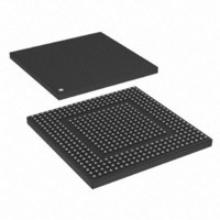
MPC8308CVMAFD Freescale Semiconductor, MPC8308CVMAFD Datasheet - Page 24

MPC8308CVMAFD
Manufacturer Part Number
MPC8308CVMAFD
Description
MPU POWERQUICC II PRO 473MAPBGA
Manufacturer
Freescale Semiconductor
Series
PowerQUICC II PROr
Datasheets
1.MPC8308VMAGD.pdf
(90 pages)
2.MPC8308VMAGD.pdf
(2 pages)
3.MPC8308VMAGD.pdf
(1170 pages)
4.MPC8308VMAGD.pdf
(14 pages)
Specifications of MPC8308CVMAFD
Processor Type
MPC83xx PowerQUICC II Pro 32-Bit
Speed
333MHz
Voltage
1V
Mounting Type
Surface Mount
Package / Case
473-MAPBGA
Product
Network Processor
Data Rate
256 bps
Frequency
333 MHz
Supply Voltage (max)
3.6 V
Supply Voltage (min)
3 V
Supply Current (max)
5 uA
Maximum Operating Temperature
+ 105 C
Minimum Operating Temperature
- 40 C
Interface
I2C, JTAG, SPI
Mounting Style
SMD/SMT
Core Size
32 Bit
Cpu Speed
333MHz
Digital Ic Case Style
MAPBGA
No. Of Pins
473
Operating Temperature Range
-40°C To +105°C
Peak Reflow Compatible (260 C)
Yes
Rohs Compliant
Yes
Leaded Process Compatible
Yes
Lead Free Status / RoHS Status
Lead free / RoHS Compliant
Features
-
Lead Free Status / Rohs Status
Lead free / RoHS Compliant
Available stocks
Company
Part Number
Manufacturer
Quantity
Price
Company:
Part Number:
MPC8308CVMAFD
Manufacturer:
Freescale Semiconductor
Quantity:
10 000
Company:
Part Number:
MPC8308CVMAFDA
Manufacturer:
Freescale Semiconductor
Quantity:
10 000
USB
9.1.2
Table 31
Figure 13
24
USB clock cycle time
Input setup to USB clock—all inputs
Input hold to USB clock—all inputs
USB clock to output valid—all outputs
Output hold from USB clock—all outputs
Notes:
1. The symbols used for timing specifications follow the pattern of t
2. All timings are in reference to USB clock.
3. All signals are measured from NVDD/2 of the rising edge of USB clock to 0.4 × NVDD of the signal in question for 3.3-V
4. Input timings are measured at the pin.
5. For purposes of active/float timing measurements, the Hi-Z or off-state is defined to be when the total current delivered
inputs and t
(US) for the input (I) to go invalid (X) with respect to the time the usb clock reference (K) goes high (H). Also, t
symbolizes usb timing (US) for the usb clock reference (K) to go high (H), with respect to the output (O) going invalid (X) or
output hold time.
signaling levels.
through the component pin is less than or equal to the leakage current specification.
lists the general timing parameters of the USB-ULPI interface.
and
USB AC Electrical Specifications
(First two letters of functional block)(reference)(state)(signal)(state)
Output Signals
USBDR_CLK
Figure 14
Input Signals
Parameter
MPC8308 PowerQUICC II Pro Processor Hardware Specification, Rev. 2
Output
provide the AC test load and signals for the USB, respectively.
t
USKHOV
Table 31. USB General Timing Parameters
Figure 13. USB AC Test Load
Z
Figure 14. USB Signals
0
= 50 Ω
t
t
USIVKH
USKHOX
Symbol
t
t
t
t
USKHOV
USKHOX
USIVKH
USIXKH
t
USCK
(First two letters of functional block)(signal)(state)(reference)(state)
for outputs. For example, t
1
R
L
= 50 Ω
t
USIXKH
Min
15
—
4
1
1
NVDD/2
USIXKH
Max
—
—
—
—
9
Freescale Semiconductor
symbolizes usb timing
Unit
ns
ns
ns
ns
ns
USKHOX
Notes
1, 2
1, 4
1, 4
1
1
for


