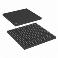
MPC8308CVMAFD Freescale Semiconductor, MPC8308CVMAFD Datasheet - Page 49

MPC8308CVMAFD
Manufacturer Part Number
MPC8308CVMAFD
Description
MPU POWERQUICC II PRO 473MAPBGA
Manufacturer
Freescale Semiconductor
Series
PowerQUICC II PROr
Datasheets
1.MPC8308VMAGD.pdf
(90 pages)
2.MPC8308VMAGD.pdf
(2 pages)
3.MPC8308VMAGD.pdf
(1170 pages)
4.MPC8308VMAGD.pdf
(14 pages)
Specifications of MPC8308CVMAFD
Processor Type
MPC83xx PowerQUICC II Pro 32-Bit
Speed
333MHz
Voltage
1V
Mounting Type
Surface Mount
Package / Case
473-MAPBGA
Product
Network Processor
Data Rate
256 bps
Frequency
333 MHz
Supply Voltage (max)
3.6 V
Supply Voltage (min)
3 V
Supply Current (max)
5 uA
Maximum Operating Temperature
+ 105 C
Minimum Operating Temperature
- 40 C
Interface
I2C, JTAG, SPI
Mounting Style
SMD/SMT
Core Size
32 Bit
Cpu Speed
333MHz
Digital Ic Case Style
MAPBGA
No. Of Pins
473
Operating Temperature Range
-40°C To +105°C
Peak Reflow Compatible (260 C)
Yes
Rohs Compliant
Yes
Leaded Process Compatible
Yes
Lead Free Status / RoHS Status
Lead free / RoHS Compliant
Features
-
Lead Free Status / Rohs Status
Lead free / RoHS Compliant
Available stocks
Company
Part Number
Manufacturer
Quantity
Price
Company:
Part Number:
MPC8308CVMAFD
Manufacturer:
Freescale Semiconductor
Quantity:
10 000
Company:
Part Number:
MPC8308CVMAFDA
Manufacturer:
Freescale Semiconductor
Quantity:
10 000
At recommended operating conditions NV
13.2
This section describes the AC electrical specifications for the eSDHC (SD/MMC) interface of the device.
Table 39
Figure
Freescale Semiconductor
SD_CLK clock frequency—full speed mode
SD_CLK clock cycle
SD_CLK clock frequency—identification mode
SD_CLK clock low time
SD_CLK clock high time
SD_CLK clock rise and fall times
Input setup times: SD_CMD, SD_DATx to SD_CLK
Input hold times: SD_CMD, SD_DATx to SD_CLK
Output valid: SD_CLK to SD_CMD, SD_DAT x valid
Output hold: SD_CLK to SD_CMD, SD_DAT x valid
SD card input setup
SD card input hold
SD card output valid
SD card output hold
Notes:
1
2
3
4
The symbols used for timing specifications herein follow the pattern of t
for inputs and t
full mode speed device timing (SFS) input (I) to go invalid (X) with respect to the clock reference (K) going to high (H). Also
t
going valid (V) or data output valid time. Note that, in general, the clock reference symbol representation is based on five letters
representing the clock of a particular functional. For rise and fall times, the latter convention is used with the appropriate letter:
R (rise) or F (fall).
Measured at capacitive load of 40 pF.
For reference only, according to the SD card specifications.
Average, for reference only.
SFSKHOV
36.
provides the eSDHC AC timing specifications for full speed mode as defined in
Output low voltage
Input high voltage
Input low voltage
eSDHC AC Timing Specifications (Full Speed Mode)
symbolizes eSDHC full speed timing (SFS) for the clock reference (K) to go high (H), with respect to the output (O)
(first three letters of functional block)(reference)(state)(signal)(state)
Characteristic
Table 38. eSDHC interface DC Electrical Characteristics (continued)
MPC8308 PowerQUICC II Pro Processor Hardware Specification, Rev. 2
Parameter
Table 39. eSDHC AC Timing Specifications for Full Speed Mode
DD
= 3.3 V ± 300 mV.
Symbol
V
V
V
OL
IH
IL
I
OL
Condition
= 3.2 mA
—
—
Symbol
t
t
t
t
t
t
t
SFSKHOV
SFSKHOX
t
SFSCKR
SFSIVKH
SFSIXKH
f
t
SFSCKH
SFSCKF
SFSCKL
f
SFSCK
SFSCK
t
SIDCK
ODLY
t
t
ISU
t
OH
IH
(first three letters of functional block)(signal)(state) (reference)(state)
for outputs. For example, t
/
1
Enhanced Secure Digital Host Controller (eSDHC)
Min
–0.3
Min
2.1
40
15
15
–3
—
—
—
—
0
0
3
2
5
5
0
NV
Max
400
25
14
—
—
—
—
—
—
—
—
—
5
3
DD
Max
0.4
0.8
SFSIXKH
+ 0.3
MHz
Unit
symbolizes eSDHC
kHz
ns
ns
ns
ns
ns
ns
ns
ns
ns
ns
ns
—
Figure 35
Unit
V
V
V
Notes
—
—
—
—
2
2
2
2
2
2
3
3
3
3
and
49


