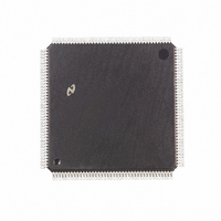
DP83907VF National Semiconductor, DP83907VF Datasheet - Page 4

DP83907VF
Manufacturer Part Number
DP83907VF
Description
IC CONTROLLR AT/LANII TP 160PQFP
Manufacturer
National Semiconductor
Datasheet
1.DP83907VF.pdf
(70 pages)
Specifications of DP83907VF
Controller Type
Network Interface Controller (NIC)
Interface
Twisted Pair
Voltage - Supply
4.75 V ~ 5.25 V
Current - Supply
150mA
Operating Temperature
0°C ~ 70°C
Mounting Type
Surface Mount
Package / Case
160-MQFP, 160-PQFP
Lead Free Status / RoHS Status
Contains lead / RoHS non-compliant
Other names
*DP83907VF
Available stocks
Company
Part Number
Manufacturer
Quantity
Price
Company:
Part Number:
DP83907VF
Manufacturer:
NSC
Quantity:
5 510
ISA BUS INTERFACE PINS
119–127
132
1 –7
10 11
15 16 18
19 21 22
24 25 98
99 101 102
104 105 107
108
118
9
8
30
13
12
29 111
112 114
115 128
129 130
2 0 Pin Description
Note Driver Types are I
AUI
Pin No
e
Attachment Unit Interface TPI
SA0–SA9
SA13–SA19
SMRD
SMWR
SD0–SD7
SD8–SD15
IOCS16
IOWR
IORD
RESET
CHRDY
AEN
IRQ3 4 5 9 10
11 12 15
Pin Name
e
Input O
e
e
Twisted Pair Interface LED
Output I O
Type
OCH
OCH
TTL
TTL
TTL
3ST
TTL
TTL
TTL
TTL
3ST
I O
O
O
O
I
I
I
I
I
I
I
e
LATCHED ADDRESS BUS Low-order 10 bits of the system’s latched 20-bit address
bus These bits are used to decode accesses to the DP83907’s I O map
LATCHED ADDRESS BUS 7 bits of the system’s latched 20-bit address bus that are
used to decode accesses to the DP83907’s boot PROM
BOOT PROM STROBES These inputs are used to access the BOOT PROM
SYSTEM DATA BUS 16-bit system data bus Used to transfer data between the
system and the DP83907
16 BIT I O TRANSFER This signal indicates that the DP83907 is responding to a 16-
bit I O access by driving 16 bits of data on the bus
I O WRITE STROBE Strobe from system to write to the DP83907’s I O map
I O READ STROBE Strobe from system to read from the DP83907’s I O map
RESET This signal is output by the system to reset all devices on the bus
CHANNEL READY This signal is used to insert wait states into system accesses
DMA ACTIVE This signal indicates that the systems DMA has control of the bus
INTERRUPT REQUEST The operation of these outputs is determined by
Configuration Register A
Bi-directional Output OCH
e
LED Drive MOS
4
e
Open Collector 3ST
e
CMOS Level Compatible XTAL
Description
e
TRI-STATE
e
Output TTL
Crystal
e
TTL Compatible


