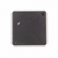
DP83907VF National Semiconductor, DP83907VF Datasheet - Page 47

DP83907VF
Manufacturer Part Number
DP83907VF
Description
IC CONTROLLR AT/LANII TP 160PQFP
Manufacturer
National Semiconductor
Datasheet
1.DP83907VF.pdf
(70 pages)
Specifications of DP83907VF
Controller Type
Network Interface Controller (NIC)
Interface
Twisted Pair
Voltage - Supply
4.75 V ~ 5.25 V
Current - Supply
150mA
Operating Temperature
0°C ~ 70°C
Mounting Type
Surface Mount
Package / Case
160-MQFP, 160-PQFP
Lead Free Status / RoHS Status
Contains lead / RoHS non-compliant
Other names
*DP83907VF
Available stocks
Company
Part Number
Manufacturer
Quantity
Price
Company:
Part Number:
DP83907VF
Manufacturer:
NSC
Quantity:
5 510
6 0 Operation of DP83907
Conditions Required to Begin Transmission
In order to transmit a packet the following three conditions
must be met
1 The Interframe Gap Timer has timed out the first 6 4 s
2 At least one byte has entered the FlFO (This indicates
3 If a collision had been detected then before transmission
In typical systems the DP83907 prefetches the first burst of
bytes before the 6 4 s timer expires The time during which
DP83907 transmits preamble can also be used to load the
FIFO
Note If carrier sense is asserted before a byte has been loaded into the
Collision Recovery
During transmission the Buffer Management logic monitors
the transmit circuitry to determine if a collision has occurred
If a collision is detected the Buffer Management logic will
reset the FlFO and restore the Transmit DMA pointers for
retransmission of the packet The COL bit will be set in the
TSR and the NCR (Number of Collisions Register) will be
incremented If 15 retransmissions each result in a collision
the transmission will be aborted and the ABT bit in the TSR
will be set
Note NCR reads as zeroes if excessive collisions are encountered
Transmit Packet Assembly Format
The following diagrams describe the format for how packets
must be assembled prior to transmission for different byte
ordering schemes The various formats are selected in the
Data Configuration Register
BOS
of the Interframe Gap
that the burst transfer has been started)
the packet time must have timed out
D15
e
FIFO the DP83907 will become a receiver
Destination Address 1
Destination Address 3
Destination Address 5
0 WTS
Source Address 1
Source Address 3
Source Address 5
Type Length 1
Data 1
e
1 in Data Configuration Register
D8
D7
Destination Address 0
Destination Address 2
Destination Address 4
Source Address 0
Source Address 2
Source Address 4
Type Length 0
Data 0
(Continued)
D0
47
This format is used with Series 32xxx or 808xx processors
BOS
This format is used with 680x0 type processors
BOS
This format is used with general 8 bit processors
Note All examples above will result in a transmission of a packet in order of
D15
e
e
DA0 DA1 DA3 bits within each byte will be transmitted least signifi-
cant bit first
DA
Destination Address 0
Destination Address 2
Destination Address 4
1 WTS
0 WTS
Source Address 0
Source Address 2
Source Address 4
e
Type Length 0
Destination Address
Data 0
e
e
1 in Data Configuration Register
D7
0 in Data Configuration Register
Destination Address 0
Destination Address 1
Destination Address 2
Destination Address 3
Destination Address 4
Destination Address 5
Source Address 0
Source Address 1
Source Address 2
Source Address 3
Source Address 4
Source Address 5
D8
D7
Destination Address 1
Destination Address 3
Destination Address 5
Source Address 1
Source Address 3
Source Address 5
Type Length 1
D0
Data 1
D0


