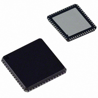
AD9959BCPZ Analog Devices Inc, AD9959BCPZ Datasheet - Page 31

AD9959BCPZ
Manufacturer Part Number
AD9959BCPZ
Description
IC DDS QUAD 10BIT DAC 56LFCSP
Manufacturer
Analog Devices Inc
Datasheet
1.AD9959BCPZ.pdf
(44 pages)
Specifications of AD9959BCPZ
Resolution (bits)
10 b
Design Resources
Phase Coherent FSK Modulator (CN0186)
Master Fclk
500MHz
Tuning Word Width (bits)
32 b
Voltage - Supply
1.71 V ~ 1.96 V
Operating Temperature
-40°C ~ 85°C
Mounting Type
Surface Mount
Package / Case
56-LFCSP
Sampling Rate
500MSPS
Input Channel Type
Serial
Supply Voltage Range - Analog
1.71V To 1.89V
Supply Current
160mA
Digital Ic Case Style
CSP
Data Interface
Serial, SPI
Lead Free Status / RoHS Status
Lead free / RoHS Compliant
Lead Free Status / RoHS Status
Lead free / RoHS Compliant, Lead free / RoHS Compliant
Available stocks
Company
Part Number
Manufacturer
Quantity
Price
Company:
Part Number:
AD9959BCPZ
Manufacturer:
ADI
Quantity:
1 648
Part Number:
AD9959BCPZ
Manufacturer:
ADI/亚德诺
Quantity:
20 000
SERIAL I/O PORT
OVERVIEW
The AD9959 serial I/O port offers multiple configurations to
provide significant flexibility. The serial I/O port offers an SPI-
compatible mode of operation that is virtually identical to the
SPI operation found in earlier Analog Devices DDS products.
The flexibility is provided by four data pins (SDIO_0, SDIO_1,
SDIO_2, SDIO_3) that allow four programmable modes of
serial I/O operation.
Three of the four data pins (SDIO_1, SDIO_2, SDIO_3) can be
used for functions other than serial I/O port operation. These pins
can also be used to initiate a ramp-up or ramp-down (RU/RD)
of the 10-bit amplitude output scalar. In addition, SDIO_3 can
be used to provide the SYNC_I/O function that resynchronizes
the serial I/O port controller if it is out of proper sequence.
The maximum speed of the serial I/O port SCLK is 200 MHz,
but the four data pins (SDIO_0, SDIO_1, SDIO_2, SDIO_3)
can be used to further increase data throughput. The maximum
data throughput using all the SDIO pins (SDIO_0, SDIO_1,
SDIO_2, SDIO_3) is 800 Mbps.
Note that all channels share Register 0x03 to Register 0x18, which
are shown in the Register Maps and Bit Descriptions section.
This address sharing enables all four DDS channels to be written
to simultaneously. For example, if a common frequency tuning
word is desired for all four channels, it can be written once
through the serial I/O port to all four channels. This is the
default mode of operation (all channels enabled). To enable
each channel to be independent, the four channel enable bits
found in the channel select register (CSR, Register 0x00) must
be used.
There are effectively four sets or copies of addresses (Register 0x03
to Register 0x18) that the channel enable bits can access to provide
channel independence. See the Descriptions for Control Registers
section for further details of programming channels that are
common to or independent from each other. To properly read
back Register 0x03 to Register 0x18, the user must enable only
one channel enable bit at a time.
Serial operation of the AD9959 occurs at the register level,
not the byte level; that is, the controller expects that all bytes
contained in the register address are accessed. The SYNC_I/O
function can be used to abort an I/O operation, thereby allowing
fewer than all bytes to be accessed. This feature can be used to
program only a part of the addressed register. Note that only
completed bytes are affected.
There are two phases to a serial communications cycle. Phase 1
is the instruction cycle, which writes the instruction byte into
the AD9959. Each bit of the instruction byte is registered on
each corresponding rising edge of SCLK. The instruction byte
defines whether the upcoming data transfer is a write or read
operation. The instruction byte contains the serial address of
the address register.
Rev. B | Page 31 of 44
Phase 2 of the I/O cycle consists of the actual data transfer
(write/read) between the serial port controller and the serial
port buffer. The number of bytes transferred during this phase
of the communication cycle is a function of the register being
accessed. The actual number of additional SCLK rising edges
required for the data transfer and instruction byte depends on
the number of bytes in the register and the serial I/O mode of
operation.
For example, when accessing Function Register 1 (FR1), which
is three bytes wide, Phase 2 of the I/O cycle requires that three
bytes be transferred. After transferring all data bytes per the
instruction byte, the communication cycle is completed for that
register.
At the completion of a communication cycle, the AD9959 serial
port controller expects the next set of rising SCLK edges to be
the instruction byte for the next communication cycle. All data
written to the AD9959 is registered on the rising edge of SCLK.
Data is read on the falling edge of SCLK (see Figure 43 through
Figure 49). The timing specifications for Figure 41 and Figure 42
are described in Table 25.
Table 25. Timing Specifications
Parameter
t
t
t
t
t
t
t
PRE
SCLK
DSU
SCLKPWH
SCLKPWL
DHLD
DV
SDIO_x
SCLK
Figure 42. Timing Diagram for Data Read for Serial I/O Port
CS
SDO (SDIO_2)
Figure 41. Setup and Hold Timing for the Serial I/O Port
SDIO_x
SCLK
Min
1.0
5.0
2.2
2.2
1.6
0
12
t
PRE
CS
t
SCLKPWH
t
Unit
ns min
ns min
ns min
ns min
ns min
ns min
ns min
DSU
t
DHLD
t
SCLK
t
SCLKPWL
Description
CS setup time
Period of serial data clock
Serial data setup time
Serial data clock pulse width high
Serial data clock pulse width low
Serial data hold time
Data valid time
t
DV
AD9959


