AD9959BCPZ Analog Devices Inc, AD9959BCPZ Datasheet - Page 36
AD9959BCPZ
Manufacturer Part Number
AD9959BCPZ
Description
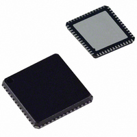
IC DDS QUAD 10BIT DAC 56LFCSP
Manufacturer
Analog Devices Inc
Datasheet
1.AD9959BCPZ.pdf
(44 pages)
Specifications of AD9959BCPZ
Resolution (bits)
10 b
Design Resources
Phase Coherent FSK Modulator (CN0186)
Master Fclk
500MHz
Tuning Word Width (bits)
32 b
Voltage - Supply
1.71 V ~ 1.96 V
Operating Temperature
-40°C ~ 85°C
Mounting Type
Surface Mount
Package / Case
56-LFCSP
Sampling Rate
500MSPS
Input Channel Type
Serial
Supply Voltage Range - Analog
1.71V To 1.89V
Supply Current
160mA
Digital Ic Case Style
CSP
Data Interface
Serial, SPI
Lead Free Status / RoHS Status
Lead free / RoHS Compliant
Lead Free Status / RoHS Status
Lead free / RoHS Compliant, Lead free / RoHS Compliant
Available stocks
Company
Part Number
Manufacturer
Quantity
Price
Company:

Part Number:
AD9959BCPZ
Manufacturer:
ADI
Quantity:
1 648
Part Number:
AD9959BCPZ
Manufacturer:
ADI/亚德诺
Quantity:
20 000


AD9959
REGISTER MAPS AND BIT DESCRIPTIONS
REGISTER MAPS
Table 28. Control Register Map
Register
Name
(Serial
Address)
Channel
Select
Register
(CSR)
(0x00)
Function
Register 1
(FR1)
(0x01)
Function
Register 2
(FR2)
(0x02)
1
In the channel select register, if the user wants four different
frequencies for all four DDS channels, use the following
protocol:
1.
2.
Channel enable bits do not require an I/O update to be activated. These bits are active immediately after the byte containing the bits is written. All other bits need an
I/O update to become active. The four channel enable bits shown in Table 28 are used to enable/disable any combination of the four channels. The default for all four
channels is enabled.
Enable (Logic 1) the Channel 0 enable bit, which is located
in the channel select register, and disable the other three
channels (Logic 0).
Write the desired frequency tuning word for Channel 0, as
described in Step 1, and then disable the Channel 0 enable
bit (Logic 0).
Bit
Range
[7:0]
[23:16]
[15:8]
[7:0]
[15:8]
[7:0]
Bit 7
(MSB)
Channel 3
enable
VCO gain
control
Open
Reference
clock input
power-down
All channels
autoclear
sweep
accumulator
Auto sync
enable
1
Bit 6
Channel 2
enable
External power-
down mode
All channels
clear sweep
accumulator
Multidevice sync
master enable
1
Profile pin configuration (PPC)[14:12]
Bit 5
Channel 1
enable
SYNC_CLK
disable
All channels
autoclear phase
accumulator
Multidevice sync
status
Rev. B | Page 36 of 44
1
PLL divider ratio[22:18]
Bit 4
Channel 0
enable
DAC reference
power-down
All channels
clear phase
accumulator
Multidevice sync
mask
3.
4.
Enable the Channel 1 enable bit only, located in the
channel select register, and disable the other three
channels.
Write the desired frequency tuning word for Channel 1 in
Step 3, then disable the Channel 1 enable bit.
1
Bit 3
Must
be 0
(RU/RD)[11:10]
Open[11:10]
ramp-down
Ramp-up/
Open[3:2]
Open[3:2]
Bit 2
Serial I/O mode
select[2:1]
Bit 1
Manual
hardware
sync
Modulation level[9:8]
Charge pump
control[17:16]
System clock
Open[9:8]
offset[1:0]
Bit 0
(LSB)
LSB first
Manual
software
sync
Default
Value
0xF0
0x00
0x00
0x00
0x00
0x00
Related parts for AD9959BCPZ
Image
Part Number
Description
Manufacturer
Datasheet
Request
R

Part Number:
Description:
BOARD EVALUATION FOR AD9959
Manufacturer:
Analog Devices Inc
Datasheet:


Part Number:
Description:
±1.7g Dual-Axis IMEMS Accelerometer Evaluation Board
Manufacturer:
Analog Devices Inc
Datasheet:

Part Number:
Description:
Inertial Sensor Evaluation System
Manufacturer:
Analog Devices Inc
Datasheet:
Part Number:
Description:
Manufacturer:
Analog Devices Inc
Datasheet:
Part Number:
Description:
Manufacturer:
Analog Devices Inc
Datasheet:
Part Number:
Description:
Manufacturer:
Analog Devices Inc
Datasheet:
Part Number:
Description:
Manufacturer:
Analog Devices Inc
Datasheet:
Part Number:
Description:
Manufacturer:
Analog Devices Inc
Datasheet:
Part Number:
Description:
Manufacturer:
Analog Devices Inc
Datasheet:
Part Number:
Description:
Manufacturer:
Analog Devices Inc
Datasheet:
Part Number:
Description:
Manufacturer:
Analog Devices Inc
Datasheet:
Part Number:
Description:
Manufacturer:
Analog Devices Inc
Datasheet: