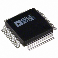
ADV7197KS Analog Devices Inc, ADV7197KS Datasheet - Page 11

ADV7197KS
Manufacturer Part Number
ADV7197KS
Description
IC DAC VID-HDTV 3CH-11BIT 52MQFP
Manufacturer
Analog Devices Inc
Type
Video Encoderr
Datasheet
1.ADV7197KS.pdf
(20 pages)
Specifications of ADV7197KS
Rohs Status
RoHS non-compliant
Applications
HDTV
Voltage - Supply, Analog
3.15 V ~ 3.45 V
Mounting Type
Surface Mount
Package / Case
52-MQFP, 52-PQFP
Adc/dac Resolution
11b
Screening Level
Industrial
Package Type
MQFP
Pin Count
52
Voltage - Supply, Digital
-
Lead Free Status / RoHS Status
Not Compliant
Available stocks
Company
Part Number
Manufacturer
Quantity
Price
Part Number:
ADV7197KS
Manufacturer:
ADI/亚德诺
Quantity:
20 000
A Logic “0” on the LSB of the first byte means that the master
will write information to the peripheral. A Logic “1” on the LSB
of the first byte means that the master will read information
from the peripheral.
The ADV7197 acts as a standard slave device on the bus. The
data on the SDA pin is 8 bits long supporting the 7-bit addresses
plus the R/W bit. It interprets the first byte as the device address
and the second byte as the starting subaddress. The subaddresses
auto-increment, allowing data to be written to or read from the
starting subaddress. A data transfer is always terminated by a
Stop condition. The user can also access any unique subad-
dress register on a one-by-one basis without having to update
all the registers.
Stop and Start conditions can be detected at any stage during the
data transfer. If these conditions are asserted out of sequence
with normal read and write operations, they cause an immediate
jump to the idle condition. During a given SCL high period the
user should issue only one Start condition, one Stop condition
or a single Stop condition followed by a single Start condition. If
an invalid subaddress is issued by the user, the ADV7197 will
not issue an acknowledge and will return to the idle condition. If
in auto-increment mode, the user exceeds the highest subaddress,
the following action will be taken:
1. In Read Mode, the highest subaddress register contents
2. In Write Mode, the data for the invalid byte will be not be
will continue to be output until the master device issues a
no-acknowledge. This indicates the end of a read. A no-
acknowledge condition is where the SDA line is not pulled
low on the ninth pulse.
loaded into any subaddress register, a no-acknowledge will
be issued by the ADV7197 and the part will return to the idle
condition.
SEQUENCE
SEQUENCE
WRITE
READ
S
S
ZERO SHOULD
S = START BIT
P = STOP BIT
BE WRITTEN
SLAVE ADDR A(S)
SLAVE ADDR A(S)
SR7
HERE
SR7
LSB = 0
SR6
A(S) = ACKNOWLEDGE BY SLAVE
A(M) = ACKNOWLEDGE BY MASTER
ADDRESS
00h
01h
02h
03h
04h
05h
06h
07h
08h
SUB ADDR
SUB ADDR
SR5
SR6 SR5
0
0
0
0
0
0
0
0
0
A(S) S SLAVE ADDR A(S)
A(S)
0
0
0
0
0
0
0
0
0
ADV7197 SUBADDRESS REGISTER
SR4
DATA
SR4
0
0
0
0
0
0
0
0
0
SR3
0
0
0
0
0
0
0
0
1
Figure 9 illustrates an example of data transfer for a read
sequence and the Start and Stop conditions.
Figure 10 shows bus write and read sequences.
REGISTER ACCESSES
The MPU can write to or read from all of the registers of the
ADV7197 except the Subaddress Registers, which are write-only
registers. The Subaddress Register determines which register is
accessed by the next read or write operation.
All communications with the part through the bus begin with an
access to the Subaddress Register. A read/write operation is
performed from/to the target address which then increments to
the next address until a Stop command on the bus is performed.
REGISTER PROGRAMMING
The following section describes the functionality of each regis-
ter. All registers can be read from as well as written to unless
otherwise stated.
Subaddress Register (SR7–SR0)
The Communications Register is an eight bit write-only register.
After the part has been accessed over the bus and a read/write
operation is selected, the subaddress is set up. The Subaddress
Register determines to/from which register the operation
takes place.
Figure 11 shows the various operations under the control of the
Subaddress Register. “0” should always be written to SR7.
Register Select (SR6–SR0)
These bits are set up to point to the required starting address.
SCLOCK
LSB = 1
A(S)
SDATA
SR3
SR2
0
0
0
0
1
1
1
1
0
A(S) = NO-ACKNOWLEDGE BY SLAVE
A(M) = NO-ACKNOWLEDGE BY MASTER
START ADDR R/W ACK SUBADDRESS ACK
SR1
0
0
1
1
0
0
1
1
0
S
DATA
SR2
SR0
0
1
0
1
0
1
0
1
0
1–7
MODE REGISTER 0
MODE REGISTER 1
MODE REGISTER 2
MODE REGISTER 3
MODE REGISTER 4
MODE REGISTER 5
COLOR Y
COLOR CR
COLOR CB
8
DATA
A(M)
SR1
9
A(S) P
1–7
SR0
8
DATA
9
A(M)
DATA
1–7
ADV7197
P
8
ACK
9
STOP
P


