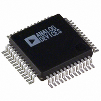
ADV7197KS Analog Devices Inc, ADV7197KS Datasheet - Page 12

ADV7197KS
Manufacturer Part Number
ADV7197KS
Description
IC DAC VID-HDTV 3CH-11BIT 52MQFP
Manufacturer
Analog Devices Inc
Type
Video Encoderr
Datasheet
1.ADV7197KS.pdf
(20 pages)
Specifications of ADV7197KS
Rohs Status
RoHS non-compliant
Applications
HDTV
Voltage - Supply, Analog
3.15 V ~ 3.45 V
Mounting Type
Surface Mount
Package / Case
52-MQFP, 52-PQFP
Adc/dac Resolution
11b
Screening Level
Industrial
Package Type
MQFP
Pin Count
52
Voltage - Supply, Digital
-
Lead Free Status / RoHS Status
Not Compliant
Available stocks
Company
Part Number
Manufacturer
Quantity
Price
Part Number:
ADV7197KS
Manufacturer:
ADI/亚德诺
Quantity:
20 000
ADV7197
MODE REGISTER 0
MR0 (MR07–MR00)
(Address (SR4–SR0) = 00H)
Figure 14 shows the various operations under the control of
Mode Register 0.
MR0 BIT DESCRIPTION
Output Standard Selection (MR00–MR01)
These bits are used to select the output levels from the ADV7197.
If EIA 770.3 (MR01–00 = “00”) is selected, the output levels will
be: 0 mV for blanking level, 700 mV for peak white (Y channel),
± 350 mV for Pr, Pb outputs and –300 mV for tri-level sync.
If Full Input Range (MR01–00 = “10”) is selected, the output
levels will be 700 mV for peak white for the Y channel, ±350 mV
for Pr, Pb outputs, and –300 mV for Sync. This mode is used
for RS-170, RS-343A standard output compatibility.
Sync insertion on the Pr, Pb channels is optional. For output
levels refer to the Appendix.
Input Control Signals (MR02–MR03)
These control bits are used to select whether data is input with
external horizontal, vertical, and blanking sync signals or if the
MR06 = ‘1’
DV SET
TSYNC
SYNC
CLK
HSYNC
VSYNC
DV
DISPLAY
81
747
A
HORIZONTAL SYNC
748
66
749
B
750
66
VERTICAL BLANKING INTERVAL
1
C
2
243
3
4
data is input with embedded EAV/SAV codes. An Asynchro-
nous timing mode is also available using TSYNC, SYNC and
DV as input control signals.
These timing control signals have to be programmed by the user
and are used for any other high definition standard input but
SMPTE274M and SMPTE296M.
Figure 12 shows an example of how to program the ADV7197
to accept a different high definition standard but SMPTE274M
or SMPTE296M.
Reserved (MR04)
A “0” must be written to this bit.
Input Standard (MR05)
Select between 1080i or 720p input.
DV Polarity (MR06)
This control bit allows to select the polarity of the DV input
control signal to be either active high or active low. This is in
order to facilitate interfacing from input devices which use an
active high blanking signal output.
Reserved (MR07)
A “0” must be written to this bit.
D
5
6
7
ACTIVE VIDEO
1920
8
25
26
27
DISPLAY
E
744
PROGRAMMABLE
INPUT TIMING
ANALOG
OUTPUT
745


