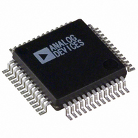
ADV7197KS Analog Devices Inc, ADV7197KS Datasheet - Page 17

ADV7197KS
Manufacturer Part Number
ADV7197KS
Description
IC DAC VID-HDTV 3CH-11BIT 52MQFP
Manufacturer
Analog Devices Inc
Type
Video Encoderr
Datasheet
1.ADV7197KS.pdf
(20 pages)
Specifications of ADV7197KS
Rohs Status
RoHS non-compliant
Applications
HDTV
Voltage - Supply, Analog
3.15 V ~ 3.45 V
Mounting Type
Surface Mount
Package / Case
52-MQFP, 52-PQFP
Adc/dac Resolution
11b
Screening Level
Industrial
Package Type
MQFP
Pin Count
52
Voltage - Supply, Digital
-
Lead Free Status / RoHS Status
Not Compliant
Available stocks
Company
Part Number
Manufacturer
Quantity
Price
Part Number:
ADV7197KS
Manufacturer:
ADI/亚德诺
Quantity:
20 000
Supply Decoupling
Noise on the analog power plane can be further reduced by the
use of decoupling capacitors.
Optimum performance is achieved by the use of 0.1 µF ceramic
capacitors. Each of group of V
vidually decoupled to ground. This should be done by placing
the capacitors as close as possible to the device with the capaci-
tor leads as short as possible, thus minimizing lead inductance.
Digital Signal Interconnect
The digital signal lines should be isolated as much as possible
from the analog outputs and other analog circuitry. Digital
signal lines should not overlay the analog power plane.
UNUSED
INPUTS
SHOULD BE
GROUNDED
V
27MHz, 74.25MHz OR
DD
74.1758MHz CLOCK
4.7k
4.7 F
6.3V
AA
or V
DD
V
pins should be indi-
AA
4.7k
Cb/Cr0–Cb/Cr9
Cr0–Cr9
Y0–Y9
HSYNC/SYNC
VSYNC/TSYNC
DV
RESET
CLKIN
COMP
ALSB
V
AA
0.1 F
ADV7197
AGND
V
AA
POWER SUPPLY DECOUPLING
FOR EACH POWER SUPPLY GROUP
26, 33
24, 35
GND
V
DAC A
DAC B
DAC C
DD
V
R
SDA
SCL
13, 52
1, 12
REF
SET
10nF
Due to the high clock rates used, long clock lines to the ADV7197
should be avoided to minimize noise pickup. Any active pull-up
termination resistors for the digital inputs should be connected
to the digital power plane and not the analog power plane.
Analog Signal Interconnect
The ADV7197 should be located as close as possible to the
output connectors thus minimizing noise pickup and reflections
due to impedance mismatch.
For optimum performance, the analog outputs should each have
a source termination resistance to ground of 75 Ω. This termi-
nation resistance should be as close as possible to the ADV7197
to minimize reflections.
Any unused inputs should be tied to ground.
10nF
300
300
300
2.47k
0.1 F
100
100
OR 2.82k
0.1 F
Y OUTPUT
Pr(V) OUTPUT
Pb(U) OUTPUT
V
V
AA
DD
V
5k
DD
V
DD
5k
MPU BUS
ADV7197


