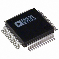
ADV7197KS Analog Devices Inc, ADV7197KS Datasheet - Page 16

ADV7197KS
Manufacturer Part Number
ADV7197KS
Description
IC DAC VID-HDTV 3CH-11BIT 52MQFP
Manufacturer
Analog Devices Inc
Type
Video Encoderr
Datasheet
1.ADV7197KS.pdf
(20 pages)
Specifications of ADV7197KS
Rohs Status
RoHS non-compliant
Applications
HDTV
Voltage - Supply, Analog
3.15 V ~ 3.45 V
Mounting Type
Surface Mount
Package / Case
52-MQFP, 52-PQFP
Adc/dac Resolution
11b
Screening Level
Industrial
Package Type
MQFP
Pin Count
52
Voltage - Supply, Digital
-
Lead Free Status / RoHS Status
Not Compliant
Available stocks
Company
Part Number
Manufacturer
Quantity
Price
Part Number:
ADV7197KS
Manufacturer:
ADI/亚德诺
Quantity:
20 000
ADV7197
COLOR Y
CY (CY7–CY0)
(Address (SR4–SR0) = 06H)
COLOR CR
CCR (CCR7–CCR0)
(Address (SR4–SR0) = 07H)
COLOR CB
CCB (CCB7–CCB0)
(Address (SR4–SR0) = 08H)
These three 8-bit-wide registers are used to program the output
color of the internal test pattern generator, be it the lines of the
cross hatch pattern or the uniform field test pattern.
The standard used for the values for Y and the color difference
signals to obtain white, black and the saturated primary and comple-
mentary colors conforms to the ITU-R BT 601-4 standard.
The Table III shows sample color values to be programmed into
the color registers.
Sample
Color
White
Black
Red
Green
Blue
Yellow
Cyan
Magenta
CCR7
CCB7
CY7
CCR6
CCB6
CY6
Table III. Sample Color Values
Figure 23. Color Cb Register
Figure 22. Color Cr Register
Color Y
Value
235 (EB)
16 (10)
81 (51)
145 (91)
41 (29)
210 (D2)
170 (AA)
106 (6A)
Figure 21. Color Y Register
CCR5
CCB5
CY5
COLOR CR VALUE
COLOR CB VALUE
COLOR Y VALUE
CCR4
CCB4
CY4
CCR7–CCR0
CCB7–CCB0
CY7–CY0
CCR3
CCB3
CY3
Color Cr
Value
128 (80)
128 (80)
240 (F0)
34 (22)
110 (6E)
146 (92)
16 (10)
222 (DE)
CCR2
CCB2
CY2
CCR1
CCB1
CY1
Color Cb
Value
128 (80)
128 (80)
90 (5A)
54 (36)
240 (F0)
16 (10)
166 (A6)
202 (CA)
CCR0
CCB0
CY0
–16–
DAC TERMINATION AND LAYOUT CONSIDERATIONS
Voltage Reference
The ADV7197 contains an on-board voltage reference. The
V
when the internal V
can be used with an external V
Resistor R
ground and is used to control the full scale output current and
therefore the DAC voltage output levels. For full-scale output
R
When an input range of 0–1023 is selected the value of R
must be 2820 Ω.
The ADV7197 has three analog outputs, corresponding to Y,
Pr, Pb video signals. The DACs must be used with external
buffer circuits in order to provide sufficient current to drive an
output device. A suitable op amp would be the AD8057.
PC BOARD LAYOUT CONSIDERATIONS
The ADV7197 is optimally designed for lowest noise perfor-
mance, both radiated and conducted noise. To complement the
excellent noise performance of the ADV7197, it is imperative
that great care be given to the PC board layout.
The layout should be optimized for lowest noise on the ADV7197
power and ground lines. This can be achieved by shielding the
digital inputs and providing good decoupling. The lead length
between groups of V
should be kept as short as possible to minimized inductive ringing.
It is recommended that a four-layer printed circuit board is
used. With power and ground planes separating the layer of the
signal carrying traces of the components and solder side layer.
Placement of components should consider to separate noisy
circuits, such as crystal clocks, high-speed logic circuitry and
analog circuitry.
There should be a separate analog ground plane (AGND) and
a separate digital ground plane (GND).
Power planes should encompass a digital power plane (V
analog power plane (V
the DACs and all associated circuitry, and the V
The digital power plane should contain all logic circuitry. The
analog and digital power planes should be individually connected
to the common power plane at one single point through a suit-
able filtering device, such as a ferrite bead.
DAC output traces on a PCB should be treated as transmission
lines. It is recommended that the DACs be placed as close as
possible to the output connector, with the analog output traces
being as short as possible (less than 3 inches. The DAC termi-
nation resistors should be placed as close as possible to the DAC
outputs and should overlay the PCB’s ground plane. As well as
minimizing reflections, short analog output traces will reduce
noise pickup due to neighboring digital circuitry.
REF
SET
pin is normally terminated to V
must have a value of 2470 Ω. R
SET
is connected between the R
REF
AA
AA
and AGND and V
). The analog power plane should contain
is used. Alternatively, the ADV7197
REF
(AD589).
AA
LOAD
through a 0.1 µF capacitor
has a value of 300 Ω.
DD
SET
and DGND pins
pin and analog
REF
circuitry.
DD
) and a
REV. 0
SET


