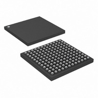
DS33X11+ Maxim Integrated Products, DS33X11+ Datasheet - Page 237

DS33X11+
Manufacturer Part Number
DS33X11+
Description
IC MAPPING ETHERNET 144CSBGA
Manufacturer
Maxim Integrated Products
Datasheet
1.DS33X11.pdf
(375 pages)
Specifications of DS33X11+
Applications
Data Transport
Interface
SPI
Voltage - Supply
1.8V, 2.5V, 3.3V
Package / Case
144-CSBGA
Mounting Type
Surface Mount
Lead Free Status / RoHS Status
Lead free / RoHS Compliant
- Current page: 237 of 375
- Download datasheet (3Mb)
303h
Default
305h:
Default
Bits 3-4: Decapsulator Add Enable (DAE[1:0]) Controls the insertion of additional bytes by the decapsulator.
Bit 2: Decapsulator GFP Synchronization Control (DGSC) When set, “triple synchronization” is selected. Three
consecutive PLIs and respective cHEC must be correct to enter the Synchronization State. If equal to zero, two
consecutive correct PLIs and cHECs are required. Only applicable to GFP Mode.
Bit 1: Decapsulator HDLC Rate Adaptation (DHRAE)
Bit 0: Decapsulator HDLC CRC Bit Order (DHCBO) Controls the endian order of the HDLC CRC calculation.
This bit function is not available in device revision A1 (GL.IDR.REVn=000).
Register Name:
Register Description:
Register Address:
302h
Default
Bits 0-15: Decapsulator 1 Data High (D1D [15:0]) These 2 bytes provide the data if the addition is enabled with
PP.DMCR.DAE[1:0].
Register Name:
Register Description:
Register Address:
304h:
Default
Bits 0-15: Decapsulator 2 Data (D2D [15:0]) These 2 bytes provide the data if the addition is enabled with
PP.DMCR.DAE[1:0].
Rev: 063008
________________________________________________ DS33X162/X161/X82/X81/X42/X41/X11/W41/W11
00 = Normal operation.
01 = The 18 byte value from the PP.DA1DR through PP.DA9DR registers will be inserted after the
10 = The 14 byte value from the PP.DA1DR through PP.DA7DR registers will be inserted after the
11 = Reserved.
0= Disabled. Default for non-X.86 (LAPS) modes.
1= Enabled. “7D DD” sequence removed from data stream. For use in X.86 (LAPS) mode.
0 = HDLC CRC will be calculated MSB-first. Default operation.
1 = HDLC CRC will be calculated LSB-first.
D1D15D
D2D15D
D1D7D
D2D7D
Bit 15
Bit 15
Bit 7
Bit 7
0
0
0
0
cHEC bytes in GFP mode, or after the HDLC header/flag when in HDLC mode.
cHEC bytes in GFP mode, or after the HDLC header/flag when in HDLC mode.
D1D14D
D2D14D
D1D6D
D2D6D
Bit 14
Bit 14
Bit 6
Bit 6
0
0
0
0
PP.DA1DR
Decapsulator Add 1 Data Register
302h (+ 040h x (n-1), WAN Group Decapsulator n=1 to 4)
PP.DA2DR
Decapsulator Add 2 Data Register
304h (+ 040h x (n-1), WAN Group Decapsulator n=1 to 4)
D1D13D
D2D13D
D1D5D
D2D5D
Bit 13
Bit 13
Bit 5
Bit 5
0
0
0
0
D1D12D
D2D12D
D1D4D
D2D4D
Bit 12
Bit 12
Bit 4
Bit 4
0
0
0
0
D1D11D
D2D11D
D1D3D
D2D3D
Bit 11
Bit 11
Bit 3
Bit 3
0
0
0
0
D1D10D
D2D10D
D1D2D
D2D2D
Bit 10
Bit 10
Bit 2
Bit 2
0
0
0
0
D1D9D
D1D1D
D2D9D
D2D1D
Bit 9
Bit 1
Bit 9
Bit 1
0
0
0
0
237 of 375
D1D8D
D1D0D
D2D8D
D2D0D
Bit 8
Bit 0
Bit 8
Bit 0
0
0
0
0
Related parts for DS33X11+
Image
Part Number
Description
Manufacturer
Datasheet
Request
R

Part Number:
Description:
MAX7528KCWPMaxim Integrated Products [CMOS Dual 8-Bit Buffered Multiplying DACs]
Manufacturer:
Maxim Integrated Products
Datasheet:

Part Number:
Description:
Single +5V, fully integrated, 1.25Gbps laser diode driver.
Manufacturer:
Maxim Integrated Products
Datasheet:

Part Number:
Description:
Single +5V, fully integrated, 155Mbps laser diode driver.
Manufacturer:
Maxim Integrated Products
Datasheet:

Part Number:
Description:
VRD11/VRD10, K8 Rev F 2/3/4-Phase PWM Controllers with Integrated Dual MOSFET Drivers
Manufacturer:
Maxim Integrated Products
Datasheet:

Part Number:
Description:
Highly Integrated Level 2 SMBus Battery Chargers
Manufacturer:
Maxim Integrated Products
Datasheet:

Part Number:
Description:
Current Monitor and Accumulator with Integrated Sense Resistor; ; Temperature Range: -40°C to +85°C
Manufacturer:
Maxim Integrated Products

Part Number:
Description:
TSSOP 14/A�/RS-485 Transceivers with Integrated 100O/120O Termination Resis
Manufacturer:
Maxim Integrated Products

Part Number:
Description:
TSSOP 14/A�/RS-485 Transceivers with Integrated 100O/120O Termination Resis
Manufacturer:
Maxim Integrated Products

Part Number:
Description:
QFN 16/A�/AC-DC and DC-DC Peak-Current-Mode Converters with Integrated Step
Manufacturer:
Maxim Integrated Products

Part Number:
Description:
TDFN/A/65V, 1A, 600KHZ, SYNCHRONOUS STEP-DOWN REGULATOR WITH INTEGRATED SWI
Manufacturer:
Maxim Integrated Products

Part Number:
Description:
Integrated Temperature Controller f
Manufacturer:
Maxim Integrated Products

Part Number:
Description:
SOT23-6/I�/45MHz to 650MHz, Integrated IF VCOs with Differential Output
Manufacturer:
Maxim Integrated Products

Part Number:
Description:
SOT23-6/I�/45MHz to 650MHz, Integrated IF VCOs with Differential Output
Manufacturer:
Maxim Integrated Products

Part Number:
Description:
EVALUATION KIT/2.4GHZ TO 2.5GHZ 802.11G/B RF TRANSCEIVER WITH INTEGRATED PA
Manufacturer:
Maxim Integrated Products

Part Number:
Description:
QFN/E/DUAL PCIE/SATA HIGH SPEED SWITCH WITH INTEGRATED BIAS RESISTOR
Manufacturer:
Maxim Integrated Products
Datasheet:


