DS33X11+ Maxim Integrated Products, DS33X11+ Datasheet - Page 339
DS33X11+
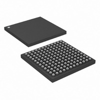
Manufacturer Part Number
DS33X11+
Description
IC MAPPING ETHERNET 144CSBGA
Manufacturer
Maxim Integrated Products
Datasheet
1.DS33X11.pdf
(375 pages)
Specifications of DS33X11+
Applications
Data Transport
Interface
SPI
Voltage - Supply
1.8V, 2.5V, 3.3V
Package / Case
144-CSBGA
Mounting Type
Surface Mount
Lead Free Status / RoHS Status
Lead free / RoHS Compliant


12.
ABSOLUTE MAXIMUM RATINGS
Voltage Range on Any Lead with respect to VSS (except VDD) ...............................–0.5V to +5.5V
Supply Voltage Range (VDD3.3) with Respect to VSS ............................................–0.3V to +3.6V
Supply Voltage Range (VDD1.8) with Respect to VSS ............................................–0.3V to +2.0V
Ambient Operating Temperature Range* ...................................................................–40ºC to +85ºC
Junction Operating Temperature Range ...................................................................–40ºC to +125ºC
Storage Temperature .................................................................................................–55ºC to +125ºC
Soldering Temperature .............................................................................................See J-STD-020 specification
These are stress ratings only and functional operation of the device at these or any other conditions beyond those indicated in the operation
sections of this specification is not implied. Exposure to absolute maximum rating conditions for extended periods of time can affect reliability.
*
test enclosure.
Note: The “typ” values listed in this document are not production tested.
Note: All A/C timing parameters are guaranteed by design.
Table 12-1. Recommended DC Operating Conditions
(VDD3.3 = 3.3V ±5%,VDD2.5 = 2.5 ± 5%, VDD1.8 = 1.8 ± 5%, T
Rev: 063008
Ambient Operating Temperature Range is assuming the device is mounted on a JEDEC standard test board in a convection cooled JEDEC
Logic 1 (Pins Other Than SDRAM)
Logic 0 (Pins Other Than SDRAM)
Logic 1, DDR SDRAM Interface
Logic 0, DDR SDRAM Interface
Supply (VDD3.3) ±5%
Supply (VDD2.5) ±5%
Supply (VDDQ) ±5%
Supply (VDD1.8) ±5%
Supply (AVDD) ±5%
VREF DDR Voltage Reference
________________________________________________ DS33X162/X161/X82/X81/X42/X41/X11/W41/W11
Operating Parameters
PARAMETER
SYMBOL
V
V
V
V
V
V
V
A
V
IHDDR
V
ILDDR
DD3.3
DD2.5
DD1.8
VREF
DDQ
VDD
IH
IL
CONDITIONS
j
= -40°C to +85°C.)
VREF +
1.1875
3.135
2.375
2.375
-0.30
-0.30
2.00
0.31
1.71
1.71
MIN
TYP
3.3
2.5
2.5
1.8
1.8
VREF –
1.3125
+0.80
2.625
3.465
2.625
2.625
MAX
0.31
1.89
1.89
5.5
339 of 375
UNITS
V
V
V
V
V
V
V
V
V
V
Related parts for DS33X11+
Image
Part Number
Description
Manufacturer
Datasheet
Request
R

Part Number:
Description:
MAX7528KCWPMaxim Integrated Products [CMOS Dual 8-Bit Buffered Multiplying DACs]
Manufacturer:
Maxim Integrated Products
Datasheet:
Part Number:
Description:
Single +5V, fully integrated, 1.25Gbps laser diode driver.
Manufacturer:
Maxim Integrated Products
Datasheet:
Part Number:
Description:
Single +5V, fully integrated, 155Mbps laser diode driver.
Manufacturer:
Maxim Integrated Products
Datasheet:
Part Number:
Description:
VRD11/VRD10, K8 Rev F 2/3/4-Phase PWM Controllers with Integrated Dual MOSFET Drivers
Manufacturer:
Maxim Integrated Products
Datasheet:
Part Number:
Description:
Highly Integrated Level 2 SMBus Battery Chargers
Manufacturer:
Maxim Integrated Products
Datasheet:
Part Number:
Description:
Current Monitor and Accumulator with Integrated Sense Resistor; ; Temperature Range: -40°C to +85°C
Manufacturer:
Maxim Integrated Products
Part Number:
Description:
TSSOP 14/A�/RS-485 Transceivers with Integrated 100O/120O Termination Resis
Manufacturer:
Maxim Integrated Products
Part Number:
Description:
TSSOP 14/A�/RS-485 Transceivers with Integrated 100O/120O Termination Resis
Manufacturer:
Maxim Integrated Products
Part Number:
Description:
QFN 16/A�/AC-DC and DC-DC Peak-Current-Mode Converters with Integrated Step
Manufacturer:
Maxim Integrated Products
Part Number:
Description:
TDFN/A/65V, 1A, 600KHZ, SYNCHRONOUS STEP-DOWN REGULATOR WITH INTEGRATED SWI
Manufacturer:
Maxim Integrated Products
Part Number:
Description:
Integrated Temperature Controller f
Manufacturer:
Maxim Integrated Products
Part Number:
Description:
SOT23-6/I�/45MHz to 650MHz, Integrated IF VCOs with Differential Output
Manufacturer:
Maxim Integrated Products
Part Number:
Description:
SOT23-6/I�/45MHz to 650MHz, Integrated IF VCOs with Differential Output
Manufacturer:
Maxim Integrated Products
Part Number:
Description:
EVALUATION KIT/2.4GHZ TO 2.5GHZ 802.11G/B RF TRANSCEIVER WITH INTEGRATED PA
Manufacturer:
Maxim Integrated Products
Part Number:
Description:
QFN/E/DUAL PCIE/SATA HIGH SPEED SWITCH WITH INTEGRATED BIAS RESISTOR
Manufacturer:
Maxim Integrated Products
Datasheet: