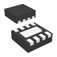
ISL29004IROZ Intersil, ISL29004IROZ Datasheet - Page 4

ISL29004IROZ
Manufacturer Part Number
ISL29004IROZ
Description
IC SENSOR LIGHT-DGTL I2C 8-ODFN
Manufacturer
Intersil
Series
-r
Datasheet
1.ISL29004IROZ-EVALZ.pdf
(17 pages)
Specifications of ISL29004IROZ
Wavelength
550nm
Output Type
I²C™
Package / Case
8-WFDFN Exposed Pad
Lead Free Status / Rohs Status
Lead free / RoHS Compliant
Principles of Operation
Photodiodes
The ISL29004 contain two photodiodes. Diode1 is sensitive
to both visible and intrared light, while Diode2 is mostly
sensitive to infrared light. The spectral response of the two
diodes are independent from one another. See Figure
Spectral Response vs Wavelength in the performance curves
section. The photodiodes convert light to current. Then, the
diodes’ current outputs are converted to digital by a single
built-in integrating type 16-bit Analog-to-Digital Converter
(ADC). An I
will be converted to a digital signal. Mode0 is Diode1 only.
Mode1 is Diode2 only. Mode3 is a sequential Mode0 and
Mode1 with an internal subtract function (Diode1 - Diode2).
Analog-to-Digital Converter.
The converter is a charge-balancing integrating type 16-bit
ADC. The chosen method for conversion is best for
converting small current signals in the presense of an AC
periodic noise. A 100ms integration time, for instance, highly
rejects 50Hz and 60Hz power line noise simultaneously. See
Integration Time and Noise Rejection section.
The built-in ADC offers user flexibility in integration time or
conversion time. Two timing modes are available. Internal
Timing Mode and External Timing Mode. In Internal Timing
Mode, integration time is determined by an internal dual speed
oscillator (fosc), and the n-bit (n = 4, 8, 12,16) counter inside the
ADC. In External Timing Mode, integration time is determined
by the time between two consecutive I
commands. See External Timing Mode example. A good
balancing act of integration time and resolution depending on
the application is required for optimal results.
The ADC has four I
dynamically accomodate various lighting conditions. For
very dim conditions, the ADC can be configured at its lowest
range. For very bright conditions, the ADC can be configured
at its highest range.
Interrupt Function
The active low interrupt pin is an open drain pull-down
configuration. The interrput pin serves as an alarm or
monitoring function to determine whether the ambient light
exceeds the upper threshold or goes below the lower
threshold. The user can also configure the persistency of the
interrupt pin. This eliminates any false triggers such as noise
or sudden spikes in ambient light conditions. An unexpected
camera flash for example can be ignored by setting the
persistency to 8 integration cycles.
I
There are eight (8) 8-bit registers available inside the
ISL29004. The command and control registers define the
operation of the device. The command and control registers do
not change until the registers are overwritten.There are two 8-
bit registers that set the high and low interrupt thresholds. There
2
C Interface
2
C command mode determines which photodiode
2
C programmable range select to
4
2
C External Timing Mode
ISL29004
are four 8-bit data Read Only registers. Two bytes for the
sensor reading and another two bytes for the timer counts. The
data registers contain the ADC's latest digital output, and the
number of clock cycles in the previous integration period.
The ISL29004’s I
by pins A0 and A1. These pins can be tied or driven either
high or low. They comprise the least-significant two bits of
the I
hardwired as 100001{A1}{A0}. The four possible addresses
are therefore 44(hex) through 47(hex).
The ISL29003’s I
internally as 44(hex).
Figure 1 shows a sample one-byte read. Figure 2 shows a
sample one-byte write. Figure 3 shows a sync_iic timing
diagram sample for externally controlled integration time.
The I
either the master or the slave can drive the SDA (data) line.
Every I
start condition (SDA falling while SCL remains high). The
following byte is driven by the master, and includes the slave
address and read/write bit. The receiving device is
responsible for pulling SDA low during the
acknowledgement period.
Every I
condition (SDA rising while SCL remains high).
For more information about the I
the Philips
2
2
C address, while the 5 most-significant bits are
C bus master always drives the SCL (clock) line, while
2
2
C transaction begins with the master asserting a
C transaction ends with the master asserting a stop
®
I
2
C specification documents.
2
2
C interface slave address is pin-selectable
C interface slave address is hardwired
2
C standard, please consult
December 21, 2006
FN6221.0


