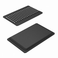
CY7C1370D-200BGXC Cypress Semiconductor Corp, CY7C1370D-200BGXC Datasheet - Page 10

CY7C1370D-200BGXC
Manufacturer Part Number
CY7C1370D-200BGXC
Description
IC SRAM 18MBIT 200MHZ 119BGA
Manufacturer
Cypress Semiconductor Corp
Type
Synchronousr
Specifications of CY7C1370D-200BGXC
Memory Size
18M (512K x 36)
Package / Case
119-BGA
Format - Memory
RAM
Memory Type
SRAM - Synchronous
Speed
200MHz
Interface
Parallel
Voltage - Supply
3.135 V ~ 3.6 V
Operating Temperature
0°C ~ 70°C
Access Time
3 ns
Maximum Clock Frequency
200 MHz
Supply Voltage (max)
3.6 V
Supply Voltage (min)
3.135 V
Maximum Operating Current
300 mA
Maximum Operating Temperature
+ 70 C
Minimum Operating Temperature
0 C
Mounting Style
SMD/SMT
Number Of Ports
4
Operating Supply Voltage
3.3 V
Lead Free Status / RoHS Status
Lead free / RoHS Compliant
Lead Free Status / RoHS Status
Lead free / RoHS Compliant, Lead free / RoHS Compliant
Available stocks
Company
Part Number
Manufacturer
Quantity
Price
Company:
Part Number:
CY7C1370D-200BGXC
Manufacturer:
Cypress Semiconductor Corp
Quantity:
10 000
Truth Table
Partial Write Cycle Description
Document Number: 38-05558 Rev. *H
Deselect cycle
Continue deselect cycle
Read cycle (begin burst)
Read cycle (continue burst)
NOP/dummy read (begin burst)
Dummy read (continue burst)
Write cycle (begin burst)
Write cycle (continue burst)
NOP/write abort (begin burst)
Write abort (continue burst)
Ignore clock edge (stall)
Sleep mode
Read
Write – No bytes written
Write byte a – (DQ
Write byte b – (DQ
Write bytes b, a
Write byte c – (DQ
Write bytes c, a
Write bytes c, b
Write bytes c, b, a
Write byte d – (DQ
Write bytes d, a
Write bytes d, b
Write bytes d, b, a
Write bytes d, c
Write bytes d, c, a
Write bytes d, c, b
Write all bytes
Notes
1. X = “Don't Care”, H = Logic HIGH, L = Logic LOW, CE stands for all chip enables active. BWx = L signifies at least one byte write select is active, BW
2. Write is defined by WE and BW
3. When a write cycle is detected, all I/Os are tri-stated, even during byte writes.
4. The DQ and DQP pins are controlled by the current cycle and the OE signal.
5. CEN = H inserts wait states.
6. Device will power-up deselected and the I/Os in a tri-state condition, regardless of OE.
7. OE is asynchronous and is not sampled with the clock rise. It is masked internally during write cycles.During a read cycle DQ
8. Table only lists a partial listing of the byte write combinations. Any Combination of BW
signifies that the desired byte write selects are asserted, see Write Cycle Description table for details.
OE is inactive or when the device is deselected, and DQ
Function (CY7C1370DV25)
Operation
[1, 2, 3, 4, 5, 6, 7]
a
b
c
d
and DQP
and DQP
and DQP
and DQP
X
. See Write Cycle Description table for details.
c
a
d
b
)
)
)
)
None
None
External
Next
External
Next
External
Next
None
Next
Current
None
Address
Used
[1, 2, 3, 8]
s
= data when OE is active.
CE
H
X
X
L
X
L
X
L
L
X
X
X
ZZ
H
L
L
L
L
L
L
L
L
L
L
L
WE
H
L
L
L
L
L
L
L
L
L
L
L
L
L
L
L
L
ADV/LD
H
H
H
H
H
X
X
L
L
L
L
L
X
is valid. Appropriate write will be done based on which byte write is active.
BW
X
H
H
H
H
H
H
H
H
L
L
L
L
L
L
L
L
WE
H
H
X
X
X
X
L
X
L
X
X
X
d
BW
H
H
X
X
X
X
X
X
L
L
X
X
x
BW
X
X
L
L
H
H
X
X
X
X
X
X
H
H
H
H
H
H
H
H
X
L
L
L
L
L
L
L
L
OE
c
L
L
L
L
L
L
L
L
L
L
H
X
CEN
s
and DQP
BW
X
H
H
H
H
H
H
H
H
L
L
L
L
L
L
L
L
L–H
L–H
L–H
L–H
L–H
L–H
L–H
L–H
L–H
L–H
L–H
X
CY7C1370DV25
CY7C1372DV25
CLK
b
X
= three-state when
Data out (Q)
Data out (Q)
Data in (D)
Data in (D)
Tri-state
Tri-state
Tri-state
Tri-state
Tri-state
Tri-state
Tri-state
Page 10 of 29
DQ
BW
–
X
H
H
H
H
H
H
H
H
L
L
L
L
L
L
L
L
x
= valid
a
[+] Feedback


