ISL97650ARTZ-T Intersil, ISL97650ARTZ-T Datasheet
ISL97650ARTZ-T
Specifications of ISL97650ARTZ-T
Available stocks


Related parts for ISL97650ARTZ-T

ISL97650ARTZ-T Summary of contents
Page 1
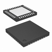
... Ordering Information PART NUMBER 27 AGND1 (Note) 26 PGND1 ISL97650ARTZ-T* 25 PGND2 ISL97650ARTZ-TK* 24 VINL *Please refer to TB347 for details on reel specifications 23 NOUT NOTE: Intersil Pb-free plus anneal products employ special Pb-free material sets; molding compounds/die attach materials and 100% 22 PGND3 matte tin plate termination finish, which are RoHS compliant and ...
Page 2
... Maximum Storage Temperature Range . . . . . . . . . .-65°C to +150°C Power Dissipation ≤ +25° .3. +70° .1. +85° .1. +100° .0.8W A Pb-Free Reflow Profile .see link below http://www.intersil.com/pbfree/Pb-FreeReflow.asp = V = 15V 25V, V BOOST SUP ON CONDITIONS Slice Positive ON Enabled, No switching IN Disabled Enabled, No switching Disabled Enabled, No Switching and VPout = V ...
Page 3
Electrical Specifications V = 12V otherwise stated. Parameters with MIN and/or MAX limits are 100% tested at +25°C, unless otherwise specified. Temperature limits established by characterization and are not production tested. (Continued) PARAMETER DESCRIPTION V Boost Output Range ...
Page 4
Electrical Specifications V = 12V otherwise stated. Parameters with MIN and/or MAX limits are 100% tested at +25°C, unless otherwise specified. Temperature limits established by characterization and are not production tested. (Continued) PARAMETER DESCRIPTION POSITIVE (V ) CHARGE ...
Page 5
Electrical Specifications V = 12V otherwise stated. Parameters with MIN and/or MAX limits are 100% tested at +25°C, unless otherwise specified. Temperature limits established by characterization and are not production tested. (Continued) PARAMETER DESCRIPTION Vth_V (FBL) V Buck ...
Page 6
Typical Performance Curves 100 500 1000 I (mA) O FIGURE 3. BUCK EFFICIENCY 0 -0.1 -0.2 -0.3 -0 -8V OFF -0.5 -0.6 -0 (mA) ...
Page 7
Typical Performance Curves Ch1 = LX(buck)(5V/DIV) Ch2 = Io(Buck)(10mA/DIV) 400ns/DIV FIGURE 9. BUCK DISCONTINUOUS MODE Ch1 = V Ch2 = LX, Ch3 = A Ch4 = I IN VDD, FIGURE 11. BOOST CONVERTER PULSE-SKIPPING MODE WAVEFORM Ch1 = V (V ...
Page 8
Pin Descriptions PIN NUMBER PIN NAME 1 LX1 2 LX2 LXL VSUP 7 FBL 8 CM2 9 CTL 10 AGND2 11 DRN 12 COM 13 POUT 14 C1- 15 C1+ 16 C2- 17 ...
Page 9
Block Diagram CM1 GM AMPLIFIER - FBB + V REF UVLO COMPARATOR - + 0.75 V REF 1.2MHz OSCILLATOR VDC1 REGULATOR IN1 IN2 EN CDEL ENL DELB V IN2 V SUP N OUT - FBN + 0.2V ...
Page 10
Typical Application Diagram V IN R18 4.7Ω VIN C1 C3 2.2µF R1 CM1 10k PGND1 4.7nF PGND2 EN BIAS AND CDEL SEQUENCE CONTROL C6 0.22µF VDC1 C18 0.47µF VDC2 C18 0.47µF C1+ C7 C1- 220nF C2+ C8 C2- 220nF VDC2 ...
Page 11
Applications Information The ISL97650 provides a complete power solution for TFT LCD applications. The system consists of one boost converter to generate A voltage for column drivers, one VDD buck converter to provide voltage to logic circuit in the LCD ...
Page 12
Boost Inductor The boost inductor is a critical part which influences the output voltage ripple, transient response, and efficiency. Values of 3.3µH to 10µH are to match the internal slope compensation. The inductor must be able to handle the following ...
Page 13
... Figure 15. The voltage rating of the external MOSFET should be greater than A VDD V IN LX1, LX2 FBB INTERSIL ISL97650 FIGURE 15. CASCADED MOSFET TOPOLOGY FOR HIGH OUTPUT VOLTAGE APPLICATIONS Buck Converter The buck converter is the step down converter, which supplies the current to the logic circuit of the LCD system. ...
Page 14
Rectifier Diode (Buck Converter) A Schottky diode is recommended due to fast recovery and low forward voltage. The reverse voltage rating should be higher than the maximum input voltage. The peak current rating is 2A, and the average current should ...
Page 15
CONTROL 1.2MHz 0.9V ERROR V REF FB In voltage doubler configuration, the maximum V given by Equations 17, 18 and 19: • – – ON_MAX(2x) SUP DIODE For Voltage Tripler: • ...
Page 16
A2 FAULT 0.4V A1 1.2MHz STOP CLK PWM EN CONTROL FIGURE 17. NEGATIVE CHARGE PUMP BLOCK DIAGRAM The maximum V output voltage of a single stage charge pump is: OFF ( ) – ...
Page 17
V CDLY REF V BOOST V LOGIC V OFF DELAYED V BOOST SLICE NOTE: Not to scale Start-Up Sequence Figure 18 shows a detailed start-up sequence waveform. For a successful power up, ...
Page 18
The delayed output appears VDD A soft-starts at the beginning of the third ramp. The VDD soft-start ramp depends on the value of the C For C of ...
Page 19
... Accordingly, the reader is cautioned to verify that data sheets are current before placing orders. Information furnished by Intersil is believed to be accurate and reliable. However, no responsibility is assumed by Intersil or its subsidiaries for its use; nor for any infringements of patents or other rights of third parties which may result from its use ...
Page 20
Package Outline Drawing L36.6x6 36 LEAD THIN QUAD FLAT NO-LEAD PLASTIC PACKAGE Rev 5, 08/08 6.00 6 PIN 1 INDEX AREA (4X) 0.15 TOP VIEW ( 5. 4.15) Exp. Dap 4.15) Exp. Dap. ( ...