ISL97650ARTZ-T Intersil, ISL97650ARTZ-T Datasheet - Page 8
ISL97650ARTZ-T
Manufacturer Part Number
ISL97650ARTZ-T
Description
IC LCD SUPPLY HP 4CHN 36-TQFN
Manufacturer
Intersil
Datasheet
1.ISL97650ARTZ-TK.pdf
(20 pages)
Specifications of ISL97650ARTZ-T
Applications
LCD TV/Monitor
Current - Supply
250µA
Voltage - Supply
4 V ~ 14 V
Operating Temperature
-40°C ~ 105°C
Mounting Type
Surface Mount
Package / Case
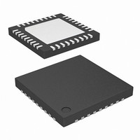
36-TQFN
Lead Free Status / RoHS Status
Lead free / RoHS Compliant
Available stocks
Company
Part Number
Manufacturer
Quantity
Price

Part Number:
ISL97650ARTZ-T
Manufacturer:
INTERSIL
Quantity:
20 000


Pin Descriptions
Exposed Die Plate
PIN NUMBER
25, 26
5, 18
10
12
13
14
15
16
17
19
20
21
22
23
24
27
28
29
30
31
32
33
34
35
36
11
1
2
3
4
6
7
8
9
PIN NAME
PGND2, 1
AGND2
PGND3
AGND1
NOUT
VSUP
POUT
VREF
VDC1
CDEL
VDC2
DELB
COM
VINL
CM2
DRN
CM1
FBP
FBN
ENL
FBB
LX1
LX2
LXL
FBL
CTL
C1+
C2+
C1-
C2-
VIN
N/A
CB
NC
EN
8
Internal boost switch connection
Internal boost switch connection
Logic buck, boost strap pin
Buck converter output
No connect. Connect to die pad and GND for improved thermal efficiency.
Positive supply for charge pumps
Logic buck feedback pin
Buck compensation network pin
Input control for V
Signal GND pin
Lower reference voltage for V
V
is connected to DRN through a 30Ω resistor
Positive charge pump out
Charge pump capacitor 1, negative connection
Charge pump capacitor 1, positive connection
Charge pump capacitor 2, negative connection
Charge pump capacitor 2, positive connection
Positive charge pump feedback pin
Reference voltage
Negative charge pump feedback pin
Power ground for V
Negative charge pump output
Logic buck supply voltage
Boost power grounds
Signal ground pin
Internal supply decoupling capacitor
Delay capacitor for start up sequencing, soft-start and fault detection timers
Buck enable for V
Open drain NFET output to drive optional A
Boost compensation network pin
Input voltage pin
Boost feedback pin
Enable for boost, charge pumps and V
Internal supply decoupling capacitor
Connect exposed die plate on rear of package to ACGND and the PGND1, 2 pins. See the section on
"“Layout Recommendation” on page 19" for PCB layout thermal considerations.
ON
slice output: when CTL = 1, COM is connected to SRC through a 5Ω resistor; when CTL = 0, COM
ON
LOGIC
OFF
slice output
ISL97650
, V
output
ON
ON
and V
slice output
ON
ON
slice
slice (independent of ENL)
DESCRIPTION
VDD
delay PFET
April 17, 2009
FN9198.4
Related parts for ISL97650ARTZ-T
Image
Part Number
Description
Manufacturer
Datasheet
Request
R

Part Number:
Description:
4-Channel Integrated LCD Supply
Manufacturer:
Intersil Corporation
Datasheet:
Part Number:
Description:
Intersil Corporation [CMOS Serial Controller Interface]
Manufacturer:
Intersil Corporation
Datasheet:
Part Number:
Description:
Manufacturer:
Intersil Corporation
Datasheet:
Part Number:
Description:
357-036-542-201 CARDEDGE 36POS DL .156 BLK LOPRO
Manufacturer:
Intersil Corporation
Datasheet:
Part Number:
Description:
1024-Word x 4-Bit LSI Static RAM
Manufacturer:
Intersil Corporation
Datasheet:
Part Number:
Description:
General Purpose NPN Transistor Arrays FN341.4
Manufacturer:
Intersil Corporation
Datasheet:
Part Number:
Description:
CMOS 16-Bit Microprocessor
Manufacturer:
Intersil Corporation
Datasheet:
Part Number:
Description:
Manufacturer:
Intersil Corporation
Datasheet:
Part Number:
Description:
Manufacturer:
Intersil Corporation
Datasheet:
Part Number:
Description:
Manufacturer:
Intersil Corporation
Datasheet:
Part Number:
Description:
Manufacturer:
Intersil Corporation
Datasheet:
Part Number:
Description:
CMOS 6-Bit Latch and Decoder Memory Interfaces
Manufacturer:
Intersil Corporation
Datasheet:
Part Number:
Description:
CA3046General Purpose NPN Transistor Arrays
Manufacturer:
Intersil Corporation
Datasheet:
Part Number:
Description:
Manufacturer:
Intersil Corporation
Datasheet:
Part Number:
Description:
TR909 DLC/FLC SLIC with Low Power Standby
Manufacturer:
Intersil Corporation
Datasheet: