ISL97650ARTZ-T Intersil, ISL97650ARTZ-T Datasheet - Page 16

ISL97650ARTZ-T
Manufacturer Part Number
ISL97650ARTZ-T
Description
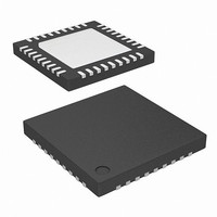
IC LCD SUPPLY HP 4CHN 36-TQFN
Manufacturer
Intersil
Datasheet
1.ISL97650ARTZ-TK.pdf
(20 pages)
Specifications of ISL97650ARTZ-T
Applications
LCD TV/Monitor
Current - Supply
250µA
Voltage - Supply
4 V ~ 14 V
Operating Temperature
-40°C ~ 105°C
Mounting Type
Surface Mount
Package / Case
36-TQFN
Lead Free Status / RoHS Status
Lead free / RoHS Compliant
Available stocks
Company
Part Number
Manufacturer
Quantity
Price
Part Number:
ISL97650ARTZ-T
Manufacturer:
INTERSIL
Quantity:
20 000
The maximum V
R6 and R7 in the “Typical Application Diagram” on page 10
determine V
Improving Charge Pump Noise Immunity
Depending on PCB layout and environment, noise pick-up at
the FBP and FBN inputs, which may degrade load regulation
performance, can be reduced by the inclusion of capacitors
across the feedback resistors (e.g. in the Application
Diagram, C21 and C22 for the positive charge pump). Set
R6 • C20 = R7 • C19 with C19 ~ 100pF.
V
The V
switching the voltage on COM between ground, DRN and SRC,
under control of the start-up sequence and the CTL pin.
During the start-up sequence, COM is held at ground via an
NDMOS FET, with ~1k impedance. Once the start-up
sequence has completed, CTL is enabled and acts as a
multiplexer control such that if CTL is low, COM connects to
DRN through a 30Ω internal MOSFET, and if CTL is high,
COM connects to P
V
V
OFF_MAX
OFF
ON
Slice Circuit
ON
=
V
Slice Circuit functions as a three way multiplexer,
FBN
(
2x
OFF
)
FAULT
•
=
⎛
⎝
OFF
1
output voltage.
–
+
V
1.2MHz
OUT
R7
------- -
R6
SUP
output voltage of a single stage charge pump is:
A2
⎞
⎠
CLK
EN
–
internally via a 5Ω MOSFET.
+
V
V
REF
DIODE
16
0.4V
STOP
•
CONTROL
⎛
⎝
R7
------- -
R6
PWM
+
2 I
⎞
⎠
A1
FIGURE 17. NEGATIVE CHARGE PUMP BLOCK DIAGRAM
•
VDD
OUT
•
(
0.2V
r
ON
(
NOUT
(EQ. 21)
(EQ. 20)
)H
M2
M1
ISL97650
VSUP
+
PGND
NOUT
r
FBN
ON
(
NOUT
820pF
The slew rate of start-up of the switch control circuit is mainly
restricted by the load capacitance at COM pin as shown in
Equation 22:
Where V
P
between COM and DRN or P
MOSFET r
inserted, R
and C
In the “Typical Application Diagram” on page 10, R10, R11
and C15 give the bias to DRN based on Equation 23:
R12 can be adjusted to adjust the slew rate.
ΔV
------- -
V
Δt
OUT
DRN
C20
)L
=
220nF
C12
)
, which range from 0V to 36V. R
------------------------------------ -
(
L
=
V
R
is the load capacitance of switch control circuit.
REF
i
g
V
-------------------------------------------------------------- -
||
ON
R
is the supply voltage applied to DRN or voltage at
DS(On)
L
V
L
g
R6
40k
is the load resistance of switch control circuit,
) C
⋅
×
R
R
11
10
L
, the trace resistance and the resistor
D3
+AVDD R
+
R
100pF
11
328k
C19
R7
D2
⋅
10
OUT
including the internal
C13
470nF
i
V
is the resistance
OFF
(-8V)
April 17, 2009
(EQ. 22)
(EQ. 23)
FN9198.4


