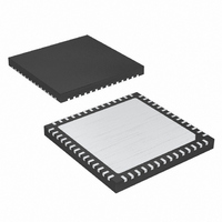
MAX8655ETN+T Maxim Integrated Products, MAX8655ETN+T Datasheet - Page 14

MAX8655ETN+T
Manufacturer Part Number
MAX8655ETN+T
Description
IC STEP-DN REG 25A 56-TQFN-EP
Manufacturer
Maxim Integrated Products
Type
Step-Down (Buck)r
Datasheet
1.MAX8655ETNT.pdf
(23 pages)
Specifications of MAX8655ETN+T
Internal Switch(s)
Yes
Synchronous Rectifier
No
Number Of Outputs
1
Voltage - Output
0.7 ~ 5.5 V
Current - Output
25A
Frequency - Switching
200kHz ~ 1MHz
Voltage - Input
4.5 ~ 25 V
Operating Temperature
-40°C ~ 85°C
Mounting Type
Surface Mount
Package / Case
56-TQFN Exposed Pad
Lead Free Status / RoHS Status
Lead free / RoHS Compliant
Power - Output
-
Lead Free Status / Rohs Status
Lead free / RoHS Compliant
Highly Integrated, 25A, Wide-Input,
Internal MOSFET, Step-Down Regulator
To set the output voltage for the MAX8655, connect FB
to the center of an external resistor-divider from the out-
put to GND (R3 and R5 of Figure 5). Select R5 between
5kΩ and 24kΩ, and then calculate R3 with the following
equation:
where V
placed as close as possible to the IC.
Figure 4. Single-Phase, 350kHz Switching, 6V to 20V Input, and 3.3V/20A Output
14
FSYNC INPUT
SYNC OUTPUT
FOR INTERNAL
OSCILLATOR
OPERATION ONLY
INPUT 6V TO 20V
POWER-OK OUTPUT
______________________________________________________________________________________
FB
CERAMIC
5 x 10µF
C1–C5
= 0.7V or V
76.8kΩ
VL
0.22µF
R8
C15
D1
R
100kΩ
3
R13
=
AVL
Setting the Output Voltage
AVL
R
5
×
REFIN
13kΩ
R14
⎛
⎜
⎝
POK
FSYNC
MODE
SYNCO
BST
GND
N.C.
LXB
PVIN
PVIN
PVIN
PVIN
PVIN
PVIN
10kΩ
Design Procedure
V
R12
V
OUT
FB
. R3 and R5 should be
−
1
R11
140kΩ
⎞
⎟
⎠
0.022µF
AVL
C13
R7
243kΩ
C12
560pF
MAX8655
R5
3.09kΩ
R6
3.09kΩ
11.5kΩ
R3
Figure 5. Setting the Output Voltage with a Resistor Voltage-
Divider
R9
71.5kΩ
11.5kΩ
R4
100pF
C10
3.57kΩ
MAX8655
R2
C8
0.22µF
VLGND
PGND
GND
GND
AVL
EN
VL
LX
LX
LX
LX
LX
LX
IN
LX
FB
C14
1µF
C18
2.2µF
C16
0.22µF
PVIN
R1
1.74kΩ
1.6mΩ
1µH
L1
0.22µF
C9
15µΩ ESR
3 x 220µF
C6–C19
R3
R5
ENABLE
INPUT
OUTPUT 3.3V
UP TO 20A
OFF
ON


