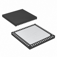
MAX8655ETN+T Maxim Integrated Products, MAX8655ETN+T Datasheet - Page 18

MAX8655ETN+T
Manufacturer Part Number
MAX8655ETN+T
Description
IC STEP-DN REG 25A 56-TQFN-EP
Manufacturer
Maxim Integrated Products
Type
Step-Down (Buck)r
Datasheet
1.MAX8655ETNT.pdf
(23 pages)
Specifications of MAX8655ETN+T
Internal Switch(s)
Yes
Synchronous Rectifier
No
Number Of Outputs
1
Voltage - Output
0.7 ~ 5.5 V
Current - Output
25A
Frequency - Switching
200kHz ~ 1MHz
Voltage - Input
4.5 ~ 25 V
Operating Temperature
-40°C ~ 85°C
Mounting Type
Surface Mount
Package / Case
56-TQFN Exposed Pad
Lead Free Status / RoHS Status
Lead free / RoHS Compliant
Power - Output
-
Lead Free Status / Rohs Status
Lead free / RoHS Compliant
Highly Integrated, 25A, Wide-Input,
Internal MOSFET, Step-Down Regulator
inductor and output capacitor resulting in a smaller
phase shift and requiring a less elaborate error-amplifier
compensation than voltage-mode control. A simple
series R
high-bandwidth loop in applications where ceramic
capacitors are used for output filtering. For other types
of capacitors, due to the higher capacitance and ESR,
the frequency of the zero created by the capacitance
and ESR is lower than the desired closed-loop crossover
frequency. To stabilize a nonceramic output-capacitor
loop, add another compensation capacitor from COMP
to GND to cancel this ESR zero. See Figure 9.
The basic regulator loop is modeled as a power modu-
lator, an output feedback divider, and an error amplifi-
er. The power modulator has DC gain G
g
the output capacitor (C
resistance (ESR). Below are equations that define the
power modulator:
where R
quency, L is the output inductance, g
R
er (12 typ), R
duty cycle D = V
factor calculated from the following equation:
When SCOMP is connected to GND, use V
when SCOMP is connected to AVL, use V
Find the pole and zero frequencies created by the
power modulator as follows:
Figure 9. Compensation Components
18
mc
L
G
), where A
f
MOD dc
pMOD
______________________________________________________________________________________
x R
(
C
LOAD
LOAD
=
and C
)
2
⎡
⎢
⎣
=
VCS
2
π
L
, with a pole and zero pair set by R
g
K
π
= V
×
mc
is the DC resistance of the inductor, the
S
MAX8655
× ×
R
C
is the gain of the current-sense amplifi-
= +
L f
OUT
OUT
LOAD
is all that is needed to have a stable,
×
1
⎡
⎢
⎣
1
S
1
1
/V
/I
120 (
+
OUT(MAX)
COMP
×
IN.
×
OUT
R
C
L f
C
V
LOAD
×
OUT
K
SCOMP
×
OUT
), and its equivalent series
S
V
S
IN
is a slope compensation
×
−
+
×
, f
[
R
R
K
[
C
V
C
S
(
× ×
C
LOAD
OUT
K
S
is the switching fre-
L f
S
× −
× −
(
SCOMP
1
)
mc
S
MOD(dc)
C
(
×
SCOMP
1
F
R
D
= 1/(A
L
)
D
−
)
)
= 2.5V.
0 5
−
.
= 1.25V;
, set by
0 5
]
LOAD
VCS
⎤
⎥
⎦
.
]
⎤
⎥
⎦
x
,
When C
lel, the resulting C
ESR
combination of like capacitors is the same as for an
individual capacitor. Figure 10 is the simplified gain
plot for the f
The feedback voltage-divider has a gain of G
V
The transconductance error amplifier has a DC gain,
G
er transconductance, which is equal to 110µS, and R
is the output resistance of the error amplifier, which is
30MΩ. A dominant pole (f
sation capacitor (C
(R
is set by the compensation resistor (R
pensation capacitor (C
(f
ESR zero if it occurs near the crossover frequency (f
Thus:
Figure 10. Simplified Gain Plot for the f zMOD > f C Case
POWER
MODULATOR
FB
pEA
EA(DC)
O
/V
), and the compensation resistor (R
(EACH)
) set by C
OUT
GAIN
(dB)
0dB
OUT
= g
, where V
/n. Note that the capacitor zero for a parallel
FB
DIVIDER
zMOD
comprises “n” identical capacitors in paral-
mEA
f
pdEA
f
F
zMOD
and R
f
f
zEA
x R
pEA
> f
OUT
FB
=
C
f
pMOD
CLOSED LOOP
C
O
2π
), the amplifier output resistance
=
=
is equal to 0.7V.
=
, where g
case.
C
2π
2π
= n x C
2π
×
C
to cancel the output capacitor
C
). There is an optional pole
×
×
pdEA
×
C
C
C
C
×
1
C
1
OUT
F
1
(
fc
1
R
×
) is set by the compen-
×
mEA
OUT(EACH)
O
R
R
f
zMOD
×
C
C
+
ESR
R
is the error-amplifi-
C
C
)
ERROR
AMPLIFIER
C
) and the com-
); a zero (f
, and ESR =
FREQUENCY
FB
zEA
C
=
O
).
)


