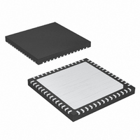
MAX8655ETN+T Maxim Integrated Products, MAX8655ETN+T Datasheet - Page 21

MAX8655ETN+T
Manufacturer Part Number
MAX8655ETN+T
Description
IC STEP-DN REG 25A 56-TQFN-EP
Manufacturer
Maxim Integrated Products
Type
Step-Down (Buck)r
Datasheet
1.MAX8655ETNT.pdf
(23 pages)
Specifications of MAX8655ETN+T
Internal Switch(s)
Yes
Synchronous Rectifier
No
Number Of Outputs
1
Voltage - Output
0.7 ~ 5.5 V
Current - Output
25A
Frequency - Switching
200kHz ~ 1MHz
Voltage - Input
4.5 ~ 25 V
Operating Temperature
-40°C ~ 85°C
Mounting Type
Surface Mount
Package / Case
56-TQFN Exposed Pad
Lead Free Status / RoHS Status
Lead free / RoHS Compliant
Power - Output
-
Lead Free Status / Rohs Status
Lead free / RoHS Compliant
Careful PCB layout is critical to achieve low losses and
clean, stable operation. Refer to the MAX8655
Evaluation Kit for an example layout. If it is necessary to
deviate from this layout, follow the procedure below.
Follow these guidelines for good PCB layout:
1) Place IC decoupling capacitors as close as possi-
2) For output current greater than 10A, a four-layer
3) Connect input, output, and VL capacitors to the
ble to the IC pins. Separate the power and analog
ground planes. Place the input ceramic decoupling
capacitor directly across and as close as possible
to PVIN and PGND. This is to help contain the high
switching current within this small loop.
PCB is recommended. Pour an analog ground
plane in the second layer underneath the IC to mini-
mize noise coupling.
power ground plane; connect all other capacitors to
the signal ground plane. Connect analog and
power ground planes at the output capacitor.
Applications Information
______________________________________________________________________________________
Internal MOSFET, Step-Down Regulator
PCB Layout Guidelines
Highly Integrated, 25A, Wide-Input,
4) Place the inductor current-sense resistor and
5) Connect the exposed pad sections to the corre-
6) Place the feedback and compensation components
PROCESS: BiCMOS
capacitor as close as possible to the inductor.
Make a Kelvin connection to minimize the effect of
PCB trace resistance. Place the input bias balance
resistor (R2 in Figure 8) near CS-. Run two closely
parallel traces from across capacitor C9 to CS+
and the input bias balance resistor R2.
sponding IC pins and allow sufficient copper area
to help cooling the device.
as close as possible to the IC pins. Connect the
feedback resistor-divider from FB to V
as possible to the farthest output capacitor.
Chip Information
OUT
as close
21


